
SERVICE MANUAL
PRINTED IN JAPAN
Oct.,2001 2
FILE NO. 050-200122
50WP16A,
50WP16C
50WP16
H, 50WP16R
50
WP16EA, 50HP81
PLASMA DISPLAY MONITOR

1 Plasma Display Technology
4
1.1. Plasma display panel
4
1.2. Plasma display panel structure
4
1.3. Rear Glass Structure
4
1.4. Front Glass Structure
4
1.5. Pixel Structure
5
1.6. Sub Field Drive system
5
1.7. Initialization
5
1.8. Write
5
1.9. Wall Voltage
6
1.10. Sustain Step 1
6
1.11. Sustain Step 2
6
1.12. Sustain Step 3
6
1.13. Sustain Step 4
7
1.14. Sustain Step 5
7
1.15. Repeat Step 1 to Step 5
7
1.16. Sub-Field drive
7
1.17. Dual Scan
8
1.18. Plasma AI (Adaptive brightness Intensifier)
8
1.19. Real Black drive
8
2 Service Hint
9
3 Adjustment Procedure
10
3.1. +B Set-up
10
3.2. Driver Set-up
10
3.3. Adjustment Volume Location
11
3.4. Test Point Location
11
3.5. Initialization Pulse Adjust
12
4 Alignment Setting
13
4.1. How to access Alignment
13
4.2. Exit
13
4.3. IIC menu structure
14
5 Alignment
16
5.1. DG contrast
16
5.2. DVCO adjust
16
5.3. NTSC panel white balance
17
5.4. PAL/SECAM panel white balance
18
5.5. Pedestal setting
20
5.6. PC/RGB panel white balance
21
5.7. HD/ 525i /525p panel white balance
23
5.8. 625i panel balance
25
5.9. Sub brighness setting
26
5.10. Pos./Size setting
28
5.11. Panel APL/ABL
28
5.12. SG Hold
28
5.13. Aging
28
5.14. LSI 33 Adjust
28
5.15. CAT (Computer Aided Test) mode
28
6SelfCheck
29
6.1. Display Indication
29
7 Trouble shooting guide
30
7.1. No Power
30
7.2. No Picture
31
7.3. Local screen failure
31
8 P.C.B. (Printed Circuit Board) exchange
32
8.1. Caution
32
8.2. Quick adjustment after P.C.B. exchange
32
9 Location of Lead Wiring
33
10 Basic Circuit Explanation
34
10.1. Power Supply Circuit
34
10.2. Energy Recovery Drive Pulse Output
35
11 IC Block Diagram
36
12 Conductor Views
39
12.1. F-Board
39
12.2. P1-Board
40
12.3. P4-Board
43
12.4. P3, P5, P6, P7, P8, P9 and T11-Board
45
12.5. H, H3, S1 and V1-Board
47
12.6. DG-Board
50
12.7. D-Board
52
12.8. C1-Board
55
12.9. C2-Board
56
12.10. C3-Board
57
12.11. C4-Board
58
12.12. C5-Board
59
12.13. C6-Board
60
12.14. C7-Board
61
12.15. C8-Board
62
12.16. SC-Board
63
12.17. SD-Board
66
12.18. SU-Board
67
12.19. SS, SS2 and SS3-Board
68
13 Block and Schematic Diagrams
71
13.1. Schematic Diagram Notes
71
13.2. Main Block Diagram
72
13.3. Power (F, P1, P3, P4, P5, P6, P7, P8 and P9 Board)
Block Diagram
73
13.4. P1-Board (1/2) Schematic Diagram
74
13.5. P1-Board (2/2) Schematic Diagram
75
13.6. P3 and P4-Board Schematic Diagram
76
13.7. P5, P6, P7 and P8-Board Schematic Diagram
77
13.8. P9 and F-Board Schematic Diagram
78
13.9. H-Board Block Diagram
79
CONTENTS
Page
Page
2

13.10. H-Board (1/4) Schematic Diagram
80
13.11. H-Board (2/4) Schematic Diagram
81
13.12. H-Board (3/4) Schematic Diagram
82
13.13. H-Board (4/4) Schematic Diagram
83
13.14. DG Board Block Diagram
84
13.15. DG-Board (1/4) Schematic Diagram
85
13.16. DG-Board (2/4) Schematic Diagram
86
13.17. DG-Board (3/4) Schematic Diagram
87
13.18. DG-Board (4/4) Schematic Diagram
88
13.19. T11 Board Schematic Diagram
89
13.20. D-Board IC Location
90
13.21. D-Board Information (1/4)
91
13.22. D-Board Information (2/4)
92
13.23. D-Board Information (3/4)
93
13.24. D-Board Information (4/4)
94
13.25. D-Board Block Diagram
95
13.26. D-Board (1/36) Schematic Diagram
96
13.27. D-Board (2/36) Schematic Diagram
97
13.28. D-Board (3/36) Schematic Diagram
98
13.29. D-Board (4/36) Schematic Diagram
99
13.30. D-Board (5/36) Schematic Diagram
100
13.31. D-Board (6/36) Schematic Diagram
101
13.32. D-Board (7/36) Schematic Diagram
102
13.33. D-Board (8/36) Schematic Diagram
103
13.34. D-Board (9/36) Schematic Diagram
104
13.35. D-Board (10/36) Schematic Diagram
105
13.36. D-Board (11/36) Schematic Diagram
106
13.37. D-Board (12/36) Schematic Diagram
107
13.38. D-Board (13/36) Schematic Diagram
108
13.39. D-Board (14/36) Schematic Diagram
109
13.40. D-Board (15/36) Schematic Diagram
110
13.41. D-Board (16/36) Schematic Diagram
111
13.42. D-Board (17/36) Schematic Diagram
112
13.43. D-Board (18/36) Schematic Diagram
113
13.44. D-Board (19/36) Schematic Diagram
114
13.45. D-Board (20/36) Schematic Diagram
115
13.46. D-Board (21/36) Schematic Diagram
116
13.47. D-Board (22/36) Schematic Diagram
117
13.48. D-Board (23/36) Schematic Diagram
118
13.49. D-Board (24/36) Schematic Diagram
119
13.50. D-Board (25/36) Schematic Diagram
120
13.51. D-Board (26/36) Schematic Diagram
121
13.52. D-Board (27/36) Schematic Diagram
122
13.53. D-Board (28/36) Schematic Diagram
123
13.54. D-Board (29/36) Schematic Diagram
124
13.55. D-Board (30/36) Schematic Diagram
125
13.56. D-Board (31/36) Schematic Diagram
126
13.57. D-Board (32/36) Schematic Diagram
127
13.58. D-Board (33/36) Schematic Diagram
128
13.59. D-Board (34/36) Schematic Diagram
129
13.60. D-Board (35/36) Schematic Diagram
130
13.61. D-Board (36/36) Schematic Diagram
131
13.62. C1, C2, C3, C4, C5, C6, C7 and C8 Board Block Diagram
132
13.63. C1-Board Schematic Diagram
133
13.64. C2-Board Schematic Diagram
134
13.65. C3-Board Schematic Diagram
135
13.66. C4-Board and V1-Board Schematic Diagram
136
13.67. C5-Board Schematic Diagram
137
13.68. C6-Board Schematic Diagram
138
13.69. C7-Board Schematic Diagram
139
13.70. C8-Board Schematic Diagram
140
13.71. SC-Board Block Diagram
141
13.72. SC-Board (1/2) Schematic Diagram
142
13.73. SC-Board (2/2) Schematic Diagram
143
13.74. SD-Board (1/2) Schematic Diagram
144
13.75. SD-Board (2/2) Schematic Diagram
145
13.76. SU-Board (1/2) Schematic Diagram
146
13.77. SU-Board (2/2) Schematic Diagram
147
13.78. SS, SS2 amd SS3 Board Block
148
13.79. SS-Board (1/2) Schematic Diagram
149
13.80. SS-Board (2/2) SS2-Board, SS3-Board and S1-Board
Schematic Diagram
150
14 Panel drive signal wave form
151
15 Signal Waveform
152
16 Mechanical Parts Location
153
17 Mechanical Replacement Parts List
155
18 Replacement Parts List
156
18.1. Relpacement Parts List Notes
156
18.2. Electrical Replacement Parts List
157
19 Specifications
180
3
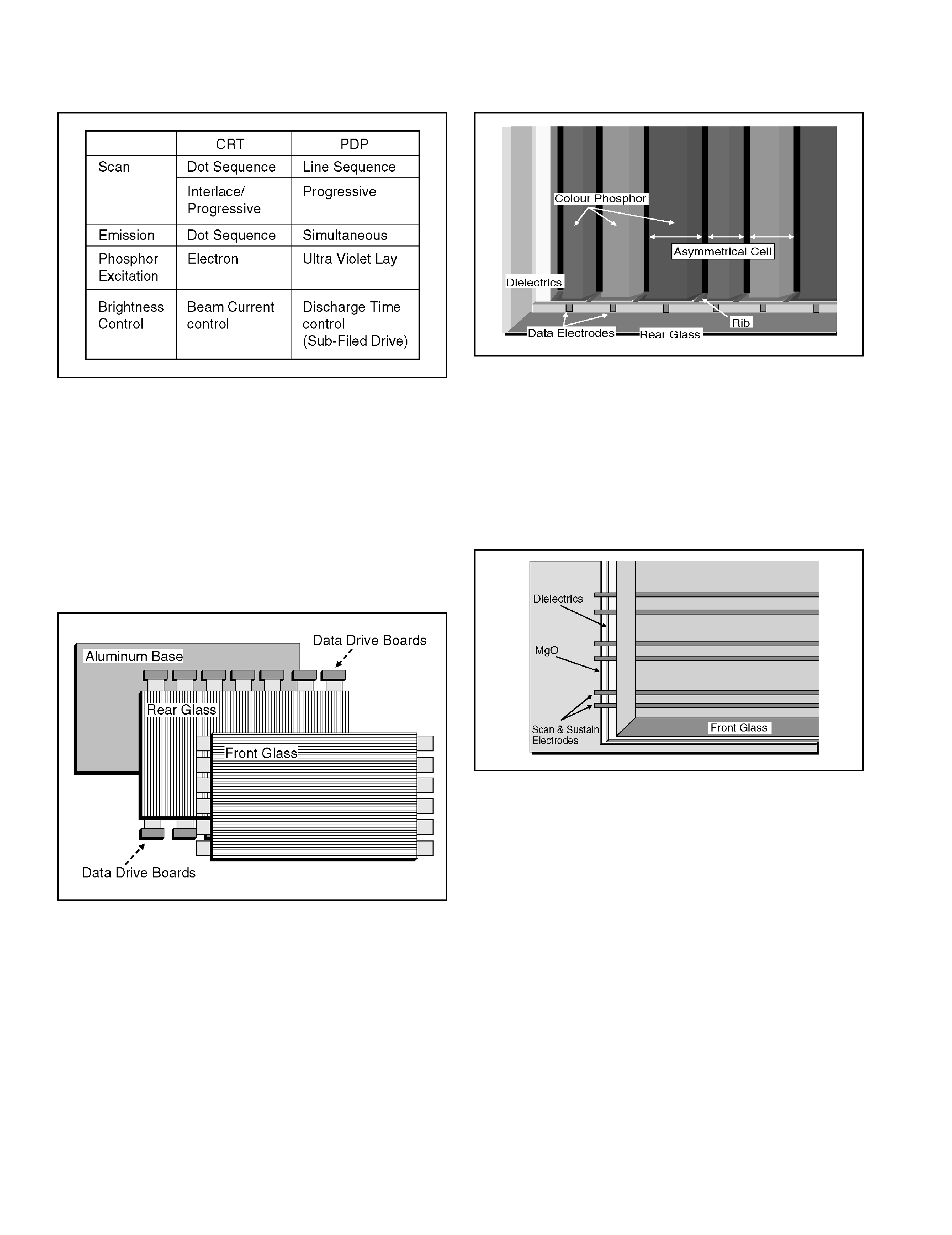
1.1.
Plasma display panel
Fig. A
Toshiba 50 wide plasma display panel is develope for large
screen multimedia display with space saving.
The plasma display panel use AC type Sub-field drive system
with Dual scanning system.
This panel have also Asymmetric cell and Plasma AI
technology.
Fig. A Is the CRT and Plasma Display Panel(PDP) comparison
chart.
1.2.
Plasma display panel structure
Fig. B
Plasma display panel structure
Plasma display panel is consist of front glass, rear glass and
Aluminum base.
The front glass has each 768 lines scan and sustain
transparence electrodes.
The rear glass has 4098 (1366 x 3 ) data electrodes on the
inner surface. These electrodes are connected to the data drive
circuit boards directory.
1.3.
Rear Glass Structure
Fig. C
On the rear glass the data electrode is mounted.
The dielectric is coated on the rear glass.
Red, Green and Blue colour phosphors are formed on the data
electrode with the ribs. However to improve colour reproduction
and brightness, each colour phosphors are formed different
width This is called " Asymmetrical cell ".
1.4.
Front Glass Structure
Fig. D
On the front glass scan and sustain transparent electrodes are
mounted in pair.
The dielectrics is coated on the front grass.
MgO over coat is also applied on the dielectrics.
The front and rear glasses are piled and sealed . And low
presser gas are charged between two glasses.
1 Plasma Display Technology
4
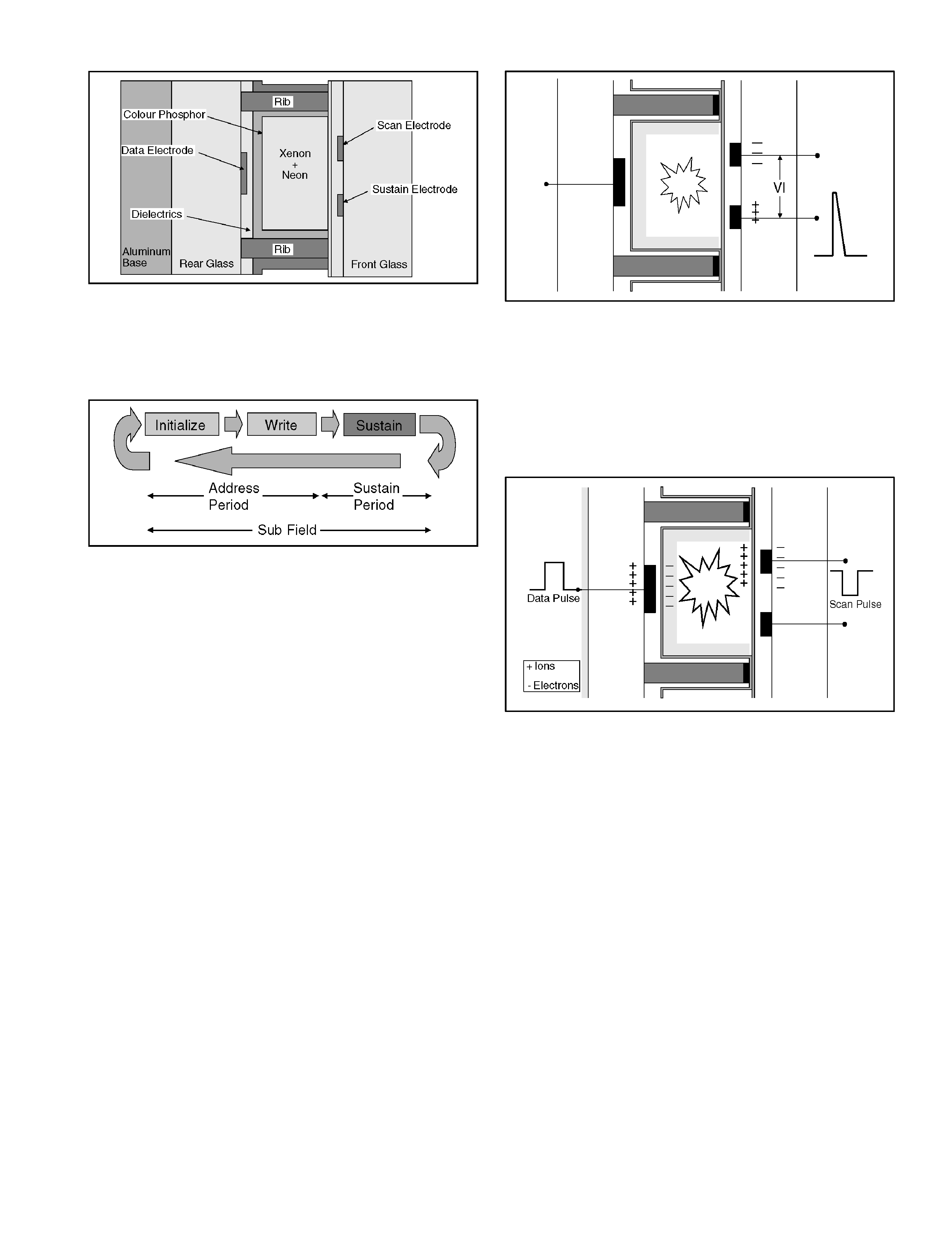
1.5.
Pixel Structure
Fig. E
50 inch plasma display panel has 1,049,088 pixels.
Each pixels structure is shown fig. E.
1.6.
Sub Field Drive system
Fig. F
Brightness control of plasma display panel is carried out by
plasma discharge time change. To control each pixelís
brightness Sub-field drive system is used.
A sub-field is consist of Initialize, Write and sustain operation.
1.7.
Initialization
Fig. G
To clear any remaining electric charge into the pixel, trapezoid
voltage is applied between the scan and sustain electrodes.
Plasma discharge is started but the discharge become small
gradually.
Then any electric charge is cleared.
1.8.
Write
Fig. H
Data Pulse which is positive polarity is input to data electrode
and Scan pulse which is negative polarity is input to scan
electrode simultaneously.
That means sum of data and scan pulses voltage is applied
between two electrodes as discharge start voltage.
Discharge is started into the pixel and gas is ionized.
During discharging Ion is charged on the scan electrode side
and electron is charged on data electrode side.
5
