TT--HH330000DDA
ABBm
mkk##
SERVICE MANUAL
DAB/AM/FM Stereo Tuner
Effective : July, 2004
S-0122A
NOTES
PC boards shown are viewed from parts side.
The parts with no reference number or no parts number in the
exploded views are not supplied.
As regards the resistors and capacitors, refer to the circuit diagrams
contained in this manual.
£
Parts marked with this sign are safety critical components. They
must be replaced with identical components - refer to the appropriate
parts list and ensure exact replacement.
CONTENTS
1 SPECIFICATIONS
2
2 MICROCOMPUTER PIN FUNCTIONS
3
3 EXPLODED VIEWS AND PARTS LIST
7
4 PC BOARDS AND PARTS LIST
9
5 INCLUDED ACCESSORIES
11
For U.K.
1 SPECIFICATIONS
2
FM Tuner
Tuning range ..........................87.50 108.00 MHz (50 kHz steps)
Signal-to-Noise ratio ................................................65 dB (Mono)
60 dB (Stereo)
AM Tuner
Tuning range ..................................522 1620 kHz (9 kHz steps)
Signal-to-Noise ratio ............................................................35 dB
DAB Tuner
Tunig range ......................................Band 3, 174 MHz 240 MHz
Input ..................................................................50 ohms, nominal
Max signal .................................................................. 3 dBm typ
Sensitivity .................................................................. 96 dBm typ
Adjacent Channel Rejection ............................................35 dB typ
Digital output ............................................24 bit/48 kHz resolution
Audio output ........................................................Stereo, 2.5 Vp-p
General
Power requirements ............................................AC 230 V, 50 Hz
Power consumption ........................................9 W (Standby: 3 W)
Dimensions (W x H x D) ..................................215 x 93 x 305 mm
Weight ..................................................................................2.3 kg
Operating temperature ................................................+5°C - +35°C
Operating humidity..........................5% to 85% (no condensation)
Storage temperature ................................................20°C - +55°C
Accessories ..................................................AM loop antenna x 1
FM Lead-type antenna x 1
DAB antenna x 1
RCA pin cable x 1
· Design and specifications are subject to change without notice.
· Weight and dimensions are approximate.
About DAB
With this unit you can receive and listen to Digital Audio
Broadcast (DAB) programmes. DAB uses digital, not analogue
signals, resulting in near CD-quality audio with virtually
interference-free reception. Along with superior quality audio,
DAB can also deliver additional audio channels and text. In the
future, computer data and images are also possible.
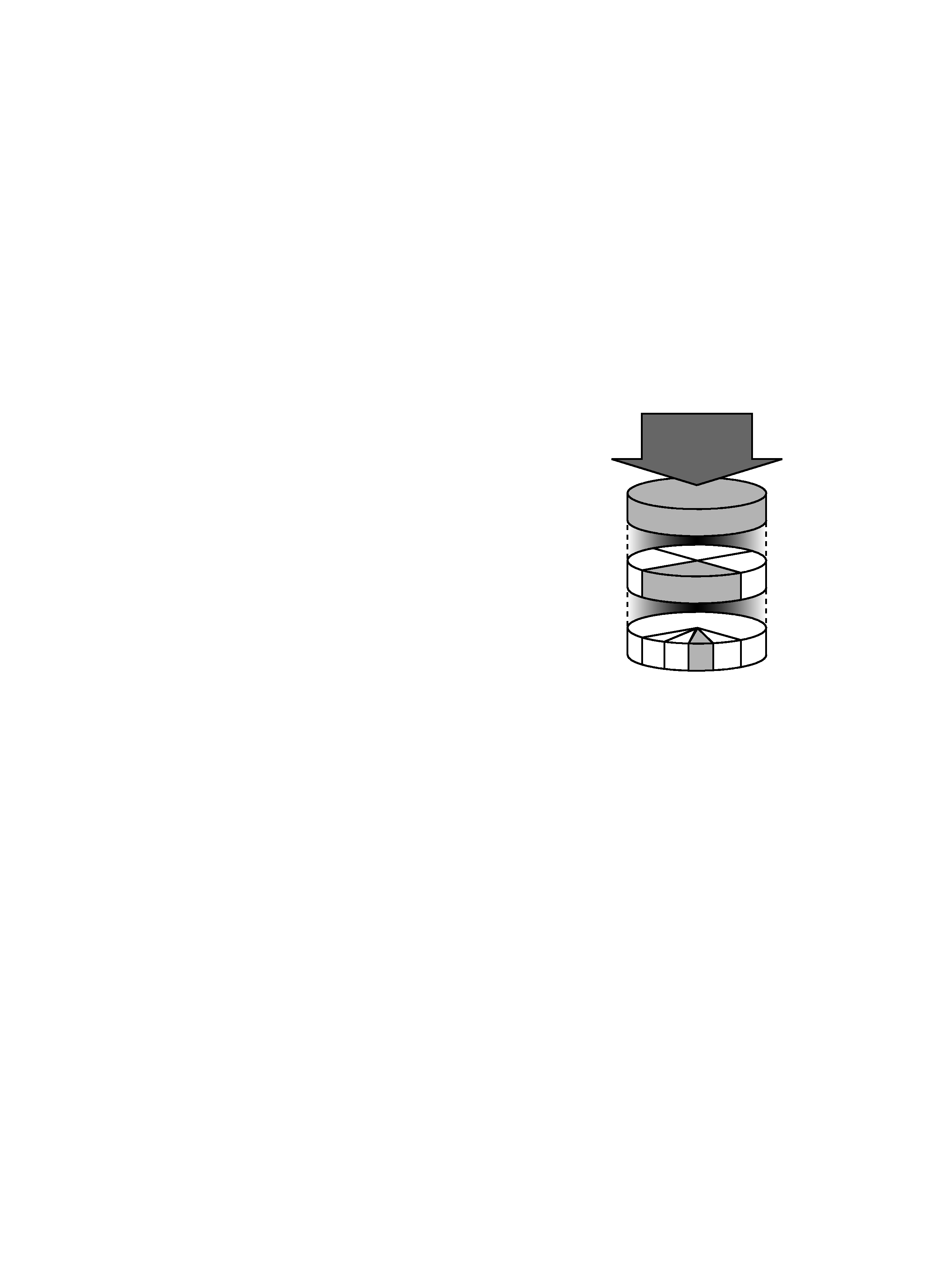
Digital radio is broadcast as groups of data called ensembles or
multiplexes. Each multiplex can contain a number of stations
(services) and each station contains a primary service and can
contain secondary services as illustrated in the following diagram.
Each multiplex is transmitted in a set frequency range and
received by this unit for decoding. You can receive multiplexes
broadcast in the 174240 MHz frequency band and store the
services in each multiplex for you to access. The number of
multiplexes you receive depend on your location. Channels used
in the UK are in the range 10A to 12D.
Multiplexes and stations have labels (names) that are used to
identify them. Instead of needing to know the particular frequency
of your favourite broadcast, you can simply select the station
name. Secondary services and additional data such as text or
multiplex info are also available.
DAB SIGNAL
MULTIPLEX
PRIMARY
SERVICES
SECONDARY
SERVICES
Parliament
BBC Radio 4
BBC
National
DAB
1
1
2
3+
1
2
3
4+
2 MICROCOMPUTER PIN FUNCTIONS
3
1
2
3
4
5
6
7
8
9
10
11
12
13
14
15
16
17
18
19
20
21
22
23
24
25
26 27 28 29 30 31 32 33 34 35 36 37 38 39 40 41 42 43 44 45 46 47 48 49 50
75
74
73
72
71
70
69
68
67
66
65
64
63
62
61
60
59
58
57
56
55
54
53
52
51
100 99 98 979695 949392 91 90898887 868584 83 82 81807978 7776
ST92F124V1
P8.4/AIN4
P8.3/AIN3
P8.2/AIN2
P8.1/AIN1/WKUP15
P8.0/AIN0/WKUP14
NC
P6.5/WKUP10/INTCLK
P6.4/NMI
P6.3/INT3/INT5
P6.2/INT2/INT4/DS2
P6.1/INT6/RW
P6.0/INT0/INT1/CLOCK2/8
P0.7/A7/D7
VDD
VSS
P0.6/A6/D6
P0.5/A5/D5
P0.3/A3/D3
P0.2/A2/D2
P0.1/A1/D1
P0.0/A0/D0
AS
DS
P0.4/A4/D4
P1.7/A15
A20/P9.6
WAIT/WKUP5/P5.0
WKUP6/WDOUT/P5.1
TXCLK/CLKOUT/P5.4
OCMPA1/P4.2
VDD
A21/P9.7
WDIN/SOUT/P5.3
DCD/WKUP8/P5.6
VSS
ICAPB1/OCMPB1/P4.3
SDA/P4.6
SIN/WKUP2/P5.2
RXCLK/WKUP7/P5.5
CLOCK2/P4.1
EXTCLK1/WKUP4/P4.4
ICAPB0/P3.1
ICAPA0/OCMPA0/P3.2
WKUP9/RTS/P5.7
ICAPA1/P4.0
EXTRG/STOUT/P4.5
WKUP1/SCL/P4.7
OCMPB0/P3.3
EXTCLK0/SS/P3.4
MISO/P3.5
P9
.5
/A1
9
P9
.4
/A1
8
P9
.2
/A1
6
HW
0S
W
1
P7
.7
/A
IN
1
5
/7
/W
K
U
P
1
3
P7
.4
/AI
N
1
2
/W
K
U
P
3
P9
.3
/A1
7
P9
.0
/R
D
I
R
ESET
P7
.6
/AI
N
1
4
/W
K
U
P
1
2
P7
.5
/AI
N
1
3
/W
K
U
P
1
1
P7
.1
/AI
N
9
P9
.1
/T
D
O
OS
C
IN
V
SS
P7
.3
/AI
N
1
1
P7
.0
/AI
N
8
/C
K_
A
F
P8
.7
/AI
N
7
OS
C
O
U
T
V
DD
P7
.2
/AI
N
1
0
AV
SS
AV
DD
P8
.6
/AI
N
6
P8
.5
/AI
N
5
MO
SI
/P3
.6
SC
K/
W
K
U
P
0
/P3
.7
RW
TO
U
T
A
0
/P
2
.2
V
SS
*V
TE
S
T
V
RE
G
TI
N
PB0
/P2
.1
TO
U
T
B
0
/P
2
.3
V
DD
V
RE
G
A
10/
P
1
.2
TI
N
PA0
/P2
.0
TI
N
PB1
/P2
.5
TO
U
T
B
1
/P
2
.7
A8
/P1
.0
A
11/
P
1
.3
A
12/
P
1
.4
TI
N
PA1
/P2
.4
TO
U
T
A
1
/P
2
.6
A9
/P1
.1
WK
U
P
6
NC
A
13/
P
1
.5
A
14/
P
1
.6
* VTEST must be kept low in standard operating mode.
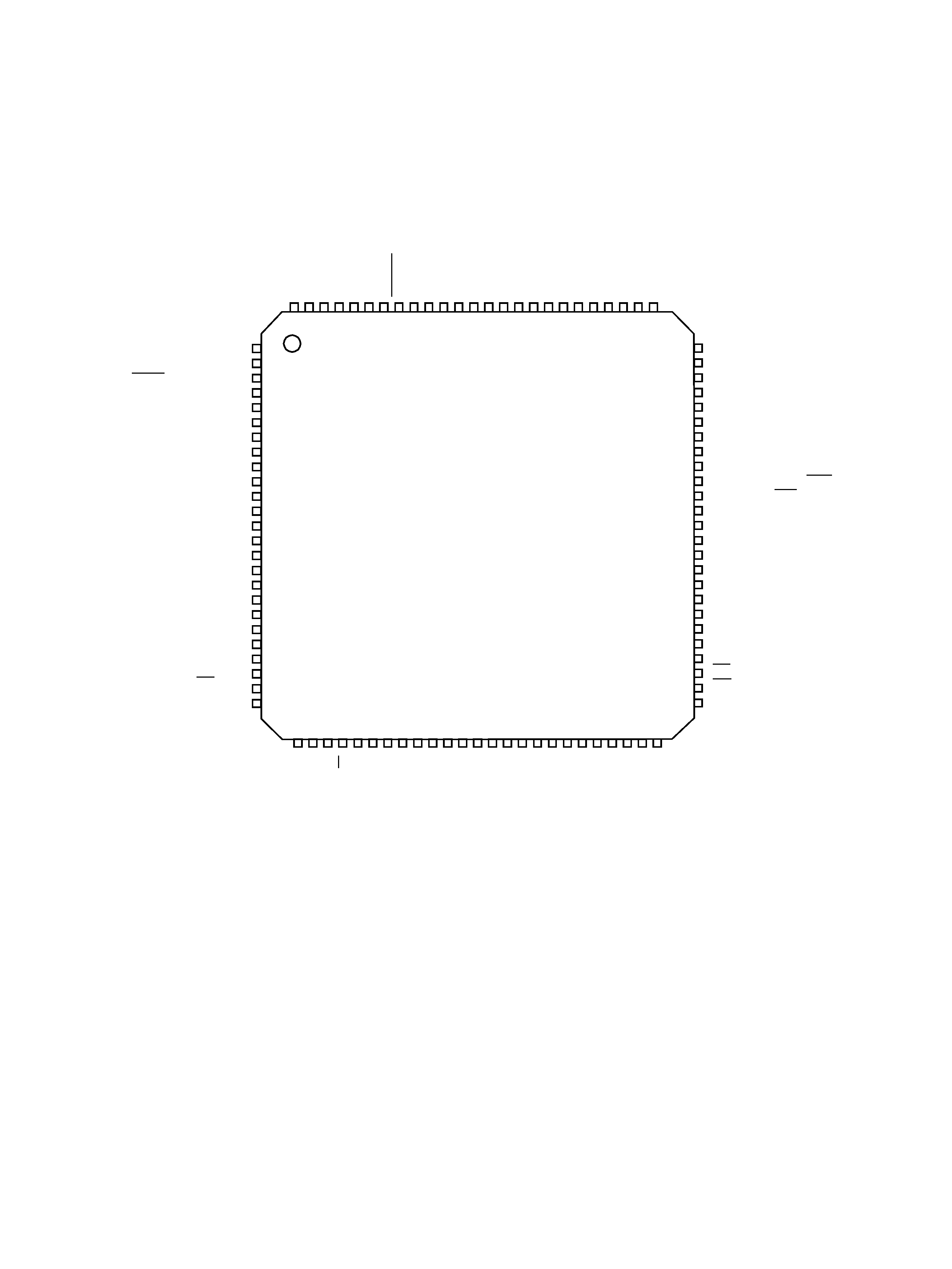
2-1 Pin Assignment
4
256 bytes
Register File
RAM
4 Kbytes
ST9 CORE
8/16 bits
CPU
Interrupt
Management
ME
MOR
Y
BU
S
RCCU
Ext. MEM.
ADDRESS
DATA
Port0
Ext. MEM.
ADDRESS
Ports
1,9
RE
GISTE
R
BU
S
WATCHDOG
AS
DS
RW
WAIT
NMI
DS2
RW
MISO
MOSI
SCK
SS
A[10:8]
A[21:11]
A[7:0]
D[7:0]
ST. TIMER
SPI
SDA
SCL
I2C BUS
FLASH
128 Kbytes
WDOUT
HW0SW1
STOUT
Fully
Prog.
I/Os
P0[7:0]
P1[7:3]
P1[2:0]
P2[7:0]
P3[7:4]
P3[3:1]
P4[7:4]
P4[3:0]
P5[7:0]
P6[5:2,0]
P6.1
P7[7:0]
P8[7:0]
P9[7:0]
MF TIMER 0
TINPA0
TOUTA0
TINPB0
TOUTB0
TINPA1
TOUTA1
TINPB1
TOUTB1
INT[6:0]
WKUP[15:0]
MF TIMER 1
E3 TM
1 Kbyte
OSCIN
OSCOUT
RESET
CLOCK2/8
INTCLK
CK_AF
ADC
AVDD
AVSS
AIN[15:8]
AIN[7:0]
EXTRG
VREG
VOLTAGE
REGULATOR
The alternate functions (
Italic characters) are mapped on Port 0, Port 1, Port2, Port3, Port4, Port5, Port6, Port7,
Port8 and Port9.
ICAPA0
OCMPA0
ICAPB0
OCMPB0
EXTCLK0
ICAPA1
OCMPA1
ICAPB1
OCMPB1
EXTCLK1
EF TIMER 0
EF TIMER 1
SCI M
TXCLK
RXCLK
SIN
DCD
SOUT
CLKOUT
RTS
SCI A
RDI
TDO
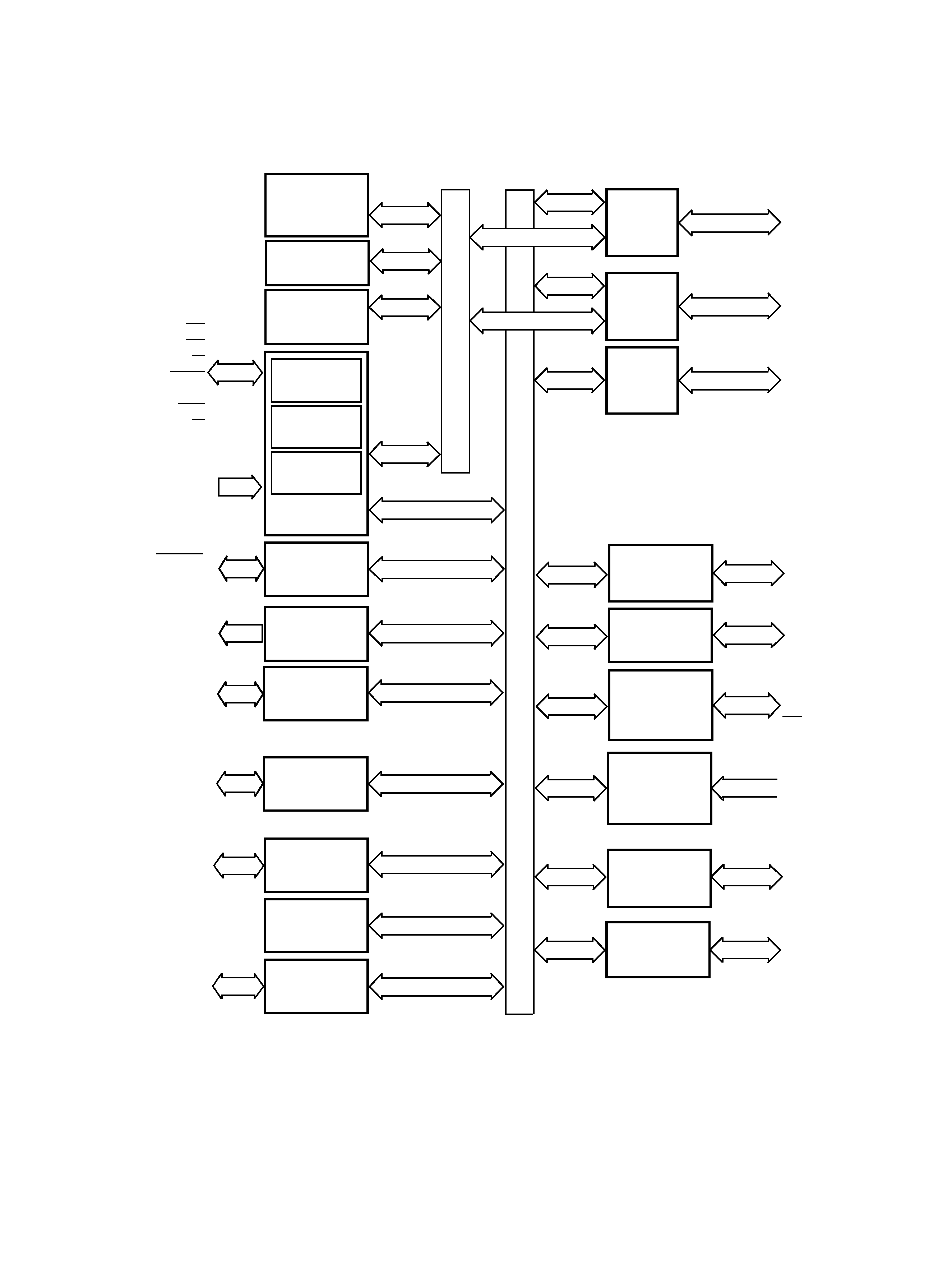
2-2 Block Diagram
5
PIN No.
NAME
I/O
DESCRIPTION
1
POWER_ON
O
Unit turn on control port ("L")
2
DAB_ON
O
DAB on control port ("L")
3
FM/AM_ON
O
FM/AM on control port ("L")
4
STAND_BY
O
Standby on control port ("L")
5
PLL_DATA
O
PLL_ Data output port
6
PLL_CLK
O
PLL_ Clock control port
7
PLL_CE
O
PLL_Chip Enable control port
8
PLL_DIN
I
PLL Data input port
9
FM/AM_MUTE
O
FM/AM MUTE control port ("L")
10
TUNED
I
Tuner module tuned control port
11
STEREO
I
Tuner module stereo control port
12
REAL_TIME_DATA
I
Real time Data port
13
REAL_TIME_CLK
I
Real time Clock Input port
14
VSS_1
-
GND
15
VDD_1
-
Power supply port (+5V)
16
RTC_OUT
O
Real time Clock Outport port
17
NC
18
DAB_DIN
I
DAB Data input port
19
DAB_DOUT
O
DAB Data output port
20
DAB_CK_OUT
O
DAB Clock output port
21
DAB_CK_IN
I
DAB Clock Input port
22~25
NC
26
RS_P
O
Register selection port
27
WRITE_ENABLE_P
O
Write enable port
28,29
NC
30
READ_ENABLE_P
O
Read enable port
31~37
NC
38
VSS_2
-
GND
39
VDD_2
-
Power supply port (+5V)
40
VREG2
-
41
V TEST
-
For Flash test purposes port ("GND")
42~44
COB0~COB2
FIP Data output port
45,46
NC
47~51
COB3~COB7
FIP Data output port
52~59
NC
60
RDS_DATA
I
RDS Data input port
61
VSS_3
-
GND
62
VDD_3
-
Power supply port (+5V)
63
BUS_OUT
O
BUS output port
64
BUS_IN
I
BUS input port
65
REMOTE_IN
I
Remote unit data input port
66
RDS_CLOCK
O
RDS Clock control port
67
BACK_UP
I
BACK_UP mode control port ("L")
68~71
NC
72
KEY 1
I
Key 1 control port
73
KEY 2
I
Key 2 control port
2-3 Pin Functions
