1
Ver 1.0 2002. 01
SERVICE MANUAL
US Model
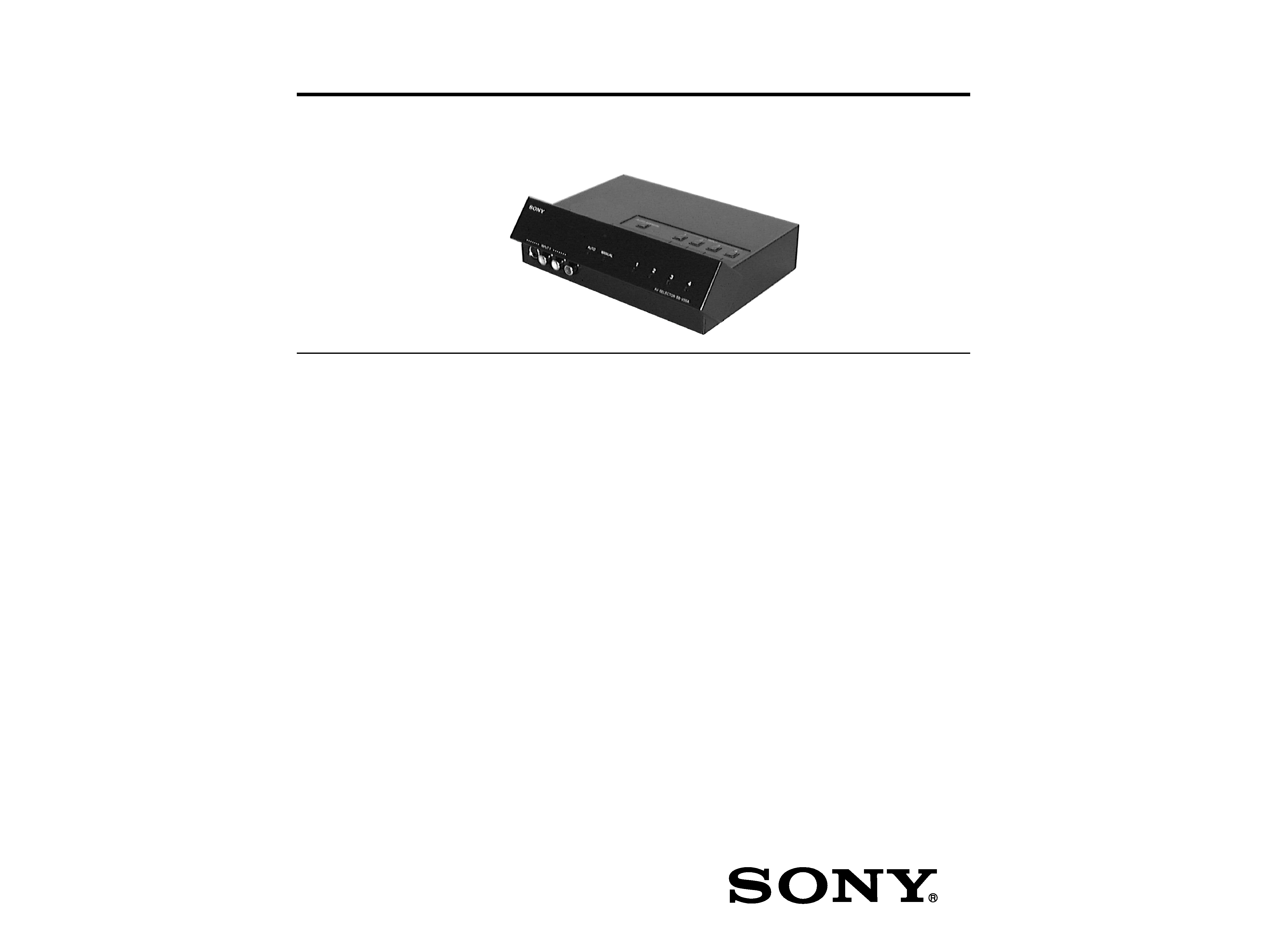
SB-V55A
AV SELECTOR
SPECIFICATIONS
Input
4 Channels
S Video, Video, Audio (L/R)
× 3
Video, Audio (L/R)
× 1
Output
S Video, Video, Audio (L/R)
× 1
Dimensions
Approx. 7 1/4
× 2 1/4 × 5 5/8 inches
(184
× 54 × 142 mm) (w/h/d)
Mass
Approx. 13 oz. (360 g)
Power
AC power adaptor
120 V AC
6 V DC
Optional accessories AC power adaptor (1)
Design and specifications are subject to change without
notice.
The "CE" printed on the unit is available only for the EU
member nations.
Sony Corporation
Personal Audio Company
Published by Sony Engineering Corporation
9-873-492-01
2002A0400-1
© 2002. 1

2
SB-V55A
TABLE OF CONTENTS
1. GENERAL
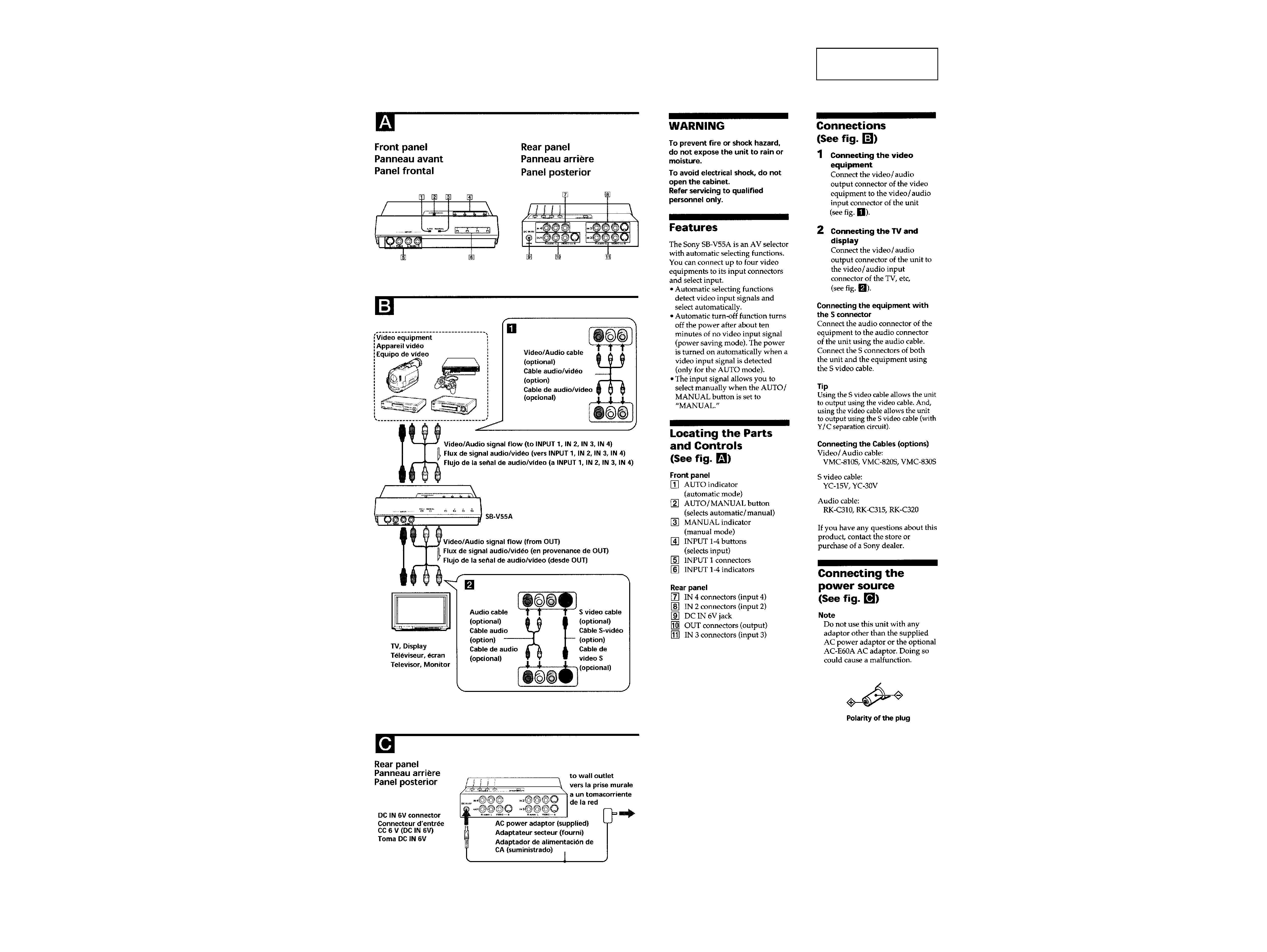
Locating the parts and controls ............................................... 3
Connections ............................................................................. 3
Connecting the power source .................................................. 3
2. DISASSEMBLY
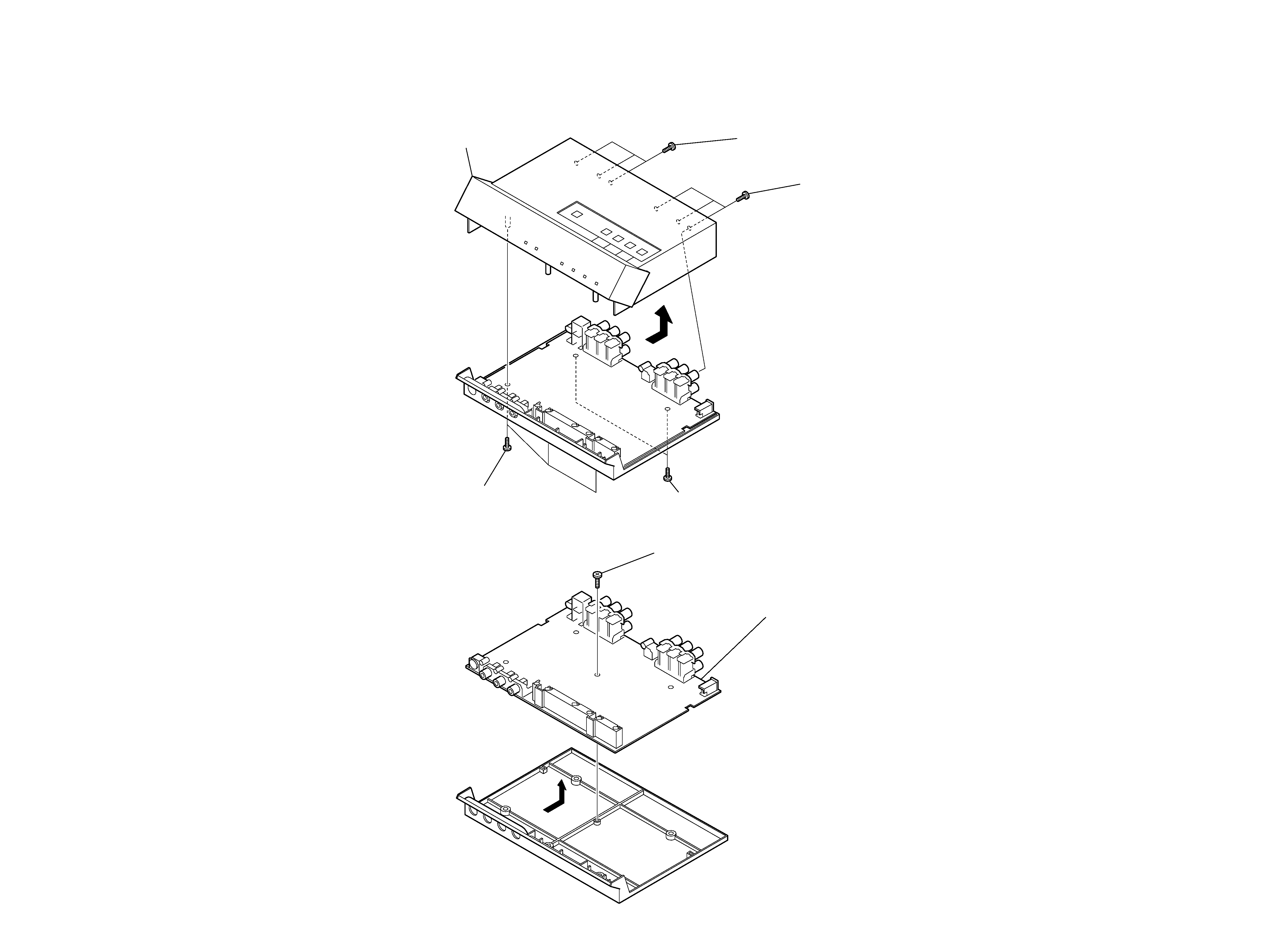
2-1. Cover, Upper ....................................................................... 4
2-2. Main Board ......................................................................... 4
3. DIAGRAMS
3-1. IC Pin Description ............................................................... 5
3-2. Block Diagram Main Section .......................................... 6
3-3. Printed Wiring Board Main Section ................................ 8
3-4. Schematic Diagram Main Section ................................. 10
4. EXPLODED VIEWS
4-1. Main Section ..................................................................... 13
5. ELECTRICAL PARTS LIST ........................................ 14
SAFETY-RELATED COMPONENT WARNING!!
COMPONENTS IDENTIFIED BY MARK 0 OR DOTTED LINE
WITH MARK 0 ON THE SCHEMATIC DIAGRAMS AND IN
THE PARTS LIST ARE CRITICAL TO SAFE OPERATION.
REPLACE THESE COMPONENTS WITH SONY PARTS WHOSE
PART NUMBERS APPEAR AS SHOWN IN THIS MANUAL OR
IN SUPPLEMENTS PUBLISHED BY SONY.
Notes on Chip Component Replacement
· Never reuse a disconnected chip component.
· Notice that the minus side of a tantalum capacitor may be dam-
aged by heat.

3
SB-V55A
SECTION 1
GENERAL
This section is extracted
from instruction manual.

4
SB-V55A
SECTION 2
DISASSEMBLY
Note : Follow the disassembly procedure in the numerical order given.
2-1. COVER, UPPER
2-2. MAIN BOARD
2
P 3x8
3
BTP 2.6x10
4
BTP 2.6x10
6
cover,upper
1
P 3x8
5
1
BTP 2.6x5
2
3
MAIN board

55
SB-V55A
3-1. IC PIN DESCRIPTION
· IC5 M34513 (SYSTEM CONTROL)
Pin No.
Pin Name
I/O
Pin Description
1
D3
O
Output port (LED (D5) light signal output in this set.)
2
D4
O
Output port (LED (D6) light signal output in this set.)
3
D5
O
Output port (LED (D7) light signal output in this set.)
4
D6/CNTR0
I/O
Clock signal input for event counter and two frequency division signal output of
under flow
5
D7/CNTR1
I/O
Clock signal input for event counter and two frequency division signal output of
under flow
6
P20/SCK
I/O
Serial clock signal input/output (Connect to ground in this set.)
7
P21/SOUT
O
Serial data signal output (Connect to ground in this set.)
8
P22/SIN
I
Serial data signal input (Connect to ground in this set.)
9
RESET
I
Reset signal input
10
CNVSS
--
Ground pin
11
XOUT
O
System clock signal output (4 MHz)
12
XIN
I
System clock signal input (4 MHz)
13
VSS
--
Ground pin
14
VDD
--
Power supply pin
15
VDCE
I
Voltage down detection signal input ("H": operate, "L": stop)
(Connect to ground in this set.)
16
P30/INT0
I/O
Input/output port and interruption signal input
17
P31/INT1
I/O
Input/output port and interruption signal input (Not used in this set.)
18
AIN0/CMP0
I
A-D convert analog signal input and voltage comparator signal input
(Connect to ground in this set.)
19
AIN1/CMP0+
I
A-D convert analog signal input and voltage comparator signal input
(Connect to ground in this set.)
20
AIN2/CMP1
I
A-D convert analog signal input and voltage comparator signal input
(Connect to ground in this set.)
21
AIN3/CMP1+
I
A-D convert analog signal input and voltage comparator signal input
(Connect to ground in this set.)
22
P00
I
Input port (Signal input of SW1 in this set.)
23
P01
I
Input port (Signal input of SW2 in this set.)
24
P02
I
Input port (Signal input of SW3 in this set.)
25
P03
I
Input port (Signal input of SW4 in this set.)
26
P10
I
Input port (Signal input of SW5 in this set.)
27
P11
I
Input port (SYNC.DET signal input in this set.)
28
P12
I/O
Input/output port (Not used in this set.)
29
P13
O
Output port (LED drive selection signal output to Q6 in this set.)
30
D0
O
Output port (LED drive selection signal output to Q5 in this set.)
31
D1
O
Output port (LED (D3) light signal output in this set.)
32
D2
O
Output port (LED (D4) light signal output in this set.)
SECTION 3
DIAGRAMS
