SERVICE MANUAL
Sony Corporation
Connect Company
Published by Sony Engineering Corporation
US Model
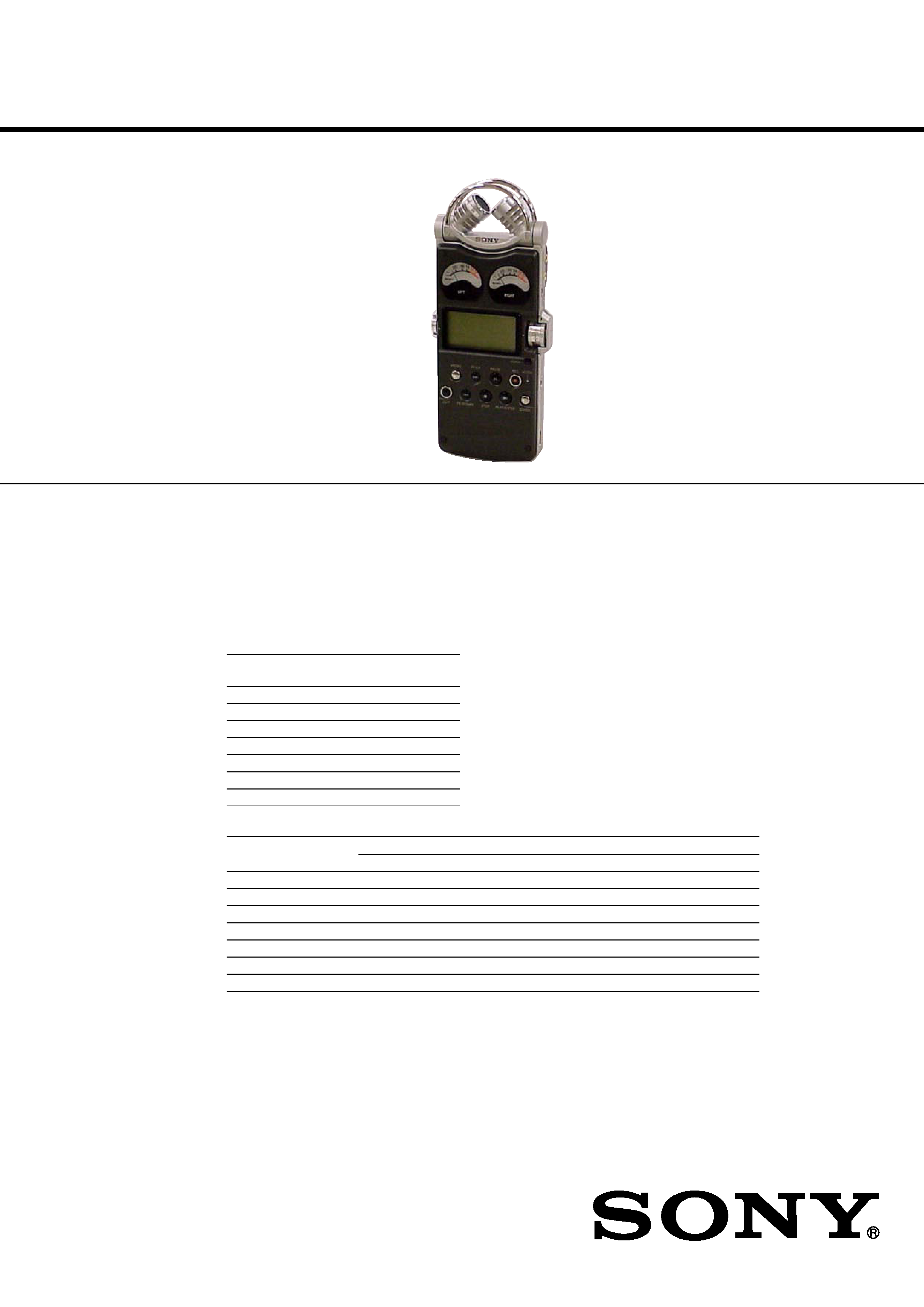
LINEAR PCM RECORDER
9-879-961-01
2005L04-1
© 2005.12
Ver. 1.0 2005.12
SPECIFICATIONS
PCM-D1
Continued on next page
Recording media
Built-in flash memory 4 GB, "Memory Stick PRO (High Speed)"
(not supplied), Stereo recording
Maximum recordable time (Approximate)
The total maximum recordable time (approximate) of all the folders is as follows.
Built-in flash memory (4 GB)
Sampling frequency/
Maximum
quantifying bit number
recordable time *
22.05 kHz 16 bit
13 hrs 10 min.
44.10 kHz 16 bit
6 hrs 35 min.
44.10 kHz 24 bit
4 hrs 20 min.
48.00 kHz 16 bit
6 hrs
48.00 kHz 24 bit
4 hrs
96.00 kHz 16 bit
3 hrs
96.00 kHz 24 bit
2 hrs
"Memory Stick PRO (High Speed)"
Sampling frequency/
Maximum recordable time *
quantifying bit number
256 MB
512 MB
1 GB
2 GB
4 GB
22.05 kHz 16 bit
45 min.
1 hr 30 min.
3 hrs 5 min.
6 hrs 25 min.
12 hrs 45 min.
44.10 kHz 16 bit
20 min.
45 min.
1 hr 30 min.
3 hrs 10 min.
6 hrs 20 min.
44.10 kHz 24 bit
15 min.
30 min.
1 hr
2 hrs 5 min.
4 hrs 15 min.
48.00 kHz 16 bit
20 min.
40 min.
1 hr 25 min.
2 hrs 55 min.
5 hrs 50 min.
48.00 kHz 24 bit
10 min.
25 min.
55 min.
1 hr 55 min.
3 hrs 50 min.
96.00 kHz 16 bit
10 min.
20 min.
40 min.
1 hr 25 min.
2 hrs 55 min.
96.00 kHz 24 bit
5 min.
10 min.
25 min.
55 min.
1 hr 55 min.
* The maximum recordable time is varied depending on recording condition.

2
PCM-D1
Quantization
16-bit linear, 24-bit linear
Frequency range (Input from the LINE IN jack
when recording/playing back) (0 to 2 dB)
Fs 22.05 kHz: 20 to 10,000 Hz
Fs 44.10 kHz: 20 to 20,000 Hz
Fs 48.00 kHz: 20 to 22,000 Hz
Fs 96.00 kHz: 20 to 44,000 Hz
Signal-to-noise ratio (S/N)
96 dB or above (1 kHz IHF-A)
(for 24 bit)
Total harmonic distortion (Input from the
LINE IN jack)
22.05 kHz 16 bit, 44.10 kHz 16/24 bit:
0.008% or below (1 kHz, 22 kHz LPF)
48.00 kHz 16/24 bit, 96.00 kHz
16/24 bit: 0.008% or below (1 kHz,
22 kHz LPF)
Wow and flutter
Below measurable limit (less than
± 0.001% W.PEAK)
Input/output
MIC jack (stereo mini jack)
Input impedance: 22k
Rated input level: 2.5mV
Minimum input level: 0.7mV
i
(headphone) jack (stereo mini jack)
Rated output level: 400mV
Maximum output level: 30mW +
30mW or more
Load impedance: 16
LINE IN jack
Input impedance: 47k
Rated input level: 2.0V
Minimum input level: 570mV
LINE OUT/optical DIGITAL OUT jack
Output impedance: 220
Rated output level: 1.8V
Load impedance: 22k
Output level: 21 to 15dBm
(for optical digital output)
Emission wavelength: 630 to 690 nm
(for optical digital output)
DC IN 6V jack
USB connector (Hi-speed USB, Mass
Storage Class)
Memory Stick slot
General
Power requirements
DC IN 6V (AC 120V, 60 Hz)
Four size AA (LR06) nickel metal
hydride rechargeable batteries NH-AA
(supplied)
Four size AA (LR06) alkaline batteries
(not supplied)
Power consumption
2.1W
Dimensions
Approx. 72.0
× 193.0 × 32.7 mm
(27/8
× 63/4 × 15/16) (w/h/d) (not
including projecting parts and
controls)
Mass
525 g (18.52 oz) (including batteries)
Supplied accessories
·Windscreen
·AC power adaptor (6V)
· USB cable
· Carrying case
For carrying the recorder and the tripod
(not supplied).
· Wrist strap
· Charging set
(Battery charger BCG-34HRE, four size AA
(LR06) nickel metal hydride rechargeable
batteries NH-AA)
· Size AA (LR06) battery case
·CD-ROM
("DigiOnSound5"*, "DigiOnAudio2
(trial version)"*, "Driver for Windows
2000")
* For instructions, refer to the help function
of each application.
· Operating Instructions (this book)
Optional accessories
"Memory Stick PRO (High Speed)"
MSX-1GN (1 GB), MSX-2GN (2 GB),
MSX-4GN (4 GB)
"Memory Stick PRO Duo (High Speed)"
MSX-M1GN (1 GB),
MSX-M2GN (2 GB)
Stereo headphones
MDR-V900, MDR-V700DJ
Audio connecting cable
RK-G129
Optical digital cable
POC-N120B (optical mini plug
y
optical mini plug)
POC-N120AB (optical mini plug
y
rectangular-shaped optical plug)
External microphone
ECM-MS957
Design and specifications are subject to change
without notice.

3
PCM-D1
SAFETY-RELATED COMPONENT WARNING!!
COMPONENTS IDENTIFIED BY MARK 0 OR DOTTED LINE
WITH MARK 0 ON THE SCHEMATIC DIAGRAMS AND IN
THE PARTS LIST ARE CRITICAL TO SAFE OPERATION.
REPLACE THESE COMPONENTS WITH SONY PARTS WHOSE
PART NUMBERS APPEAR AS SHOWN IN THIS MANUAL OR
IN SUPPLEMENTS PUBLISHED BY SONY.
Flexible Circuit Board Repairing
· Keep the temperature of the soldering iron around 270°C during
repairing.
· Do not touch the soldering iron on the same conductor of the
circuit board (within 3 times).
· Be careful not to apply force on the conductor when soldering or
unsoldering.
Notes on Chip Component Replacement
· Never reuse a disconnected chip component.
· Notice that the minus side of a tantalum capacitor may be damaged
by heat.
·UNLEADED SOLDER
Boards requiring use of unleaded solder are printed with the lead-
free mark (LF) indicating the solder contains no lead.
(Caution: Some printed circuit boards may not come printed with
the lead free mark due to their particular size.)
: LEAD FREE MARK
Unleaded solder has the following characteristics.
· Unleaded solder melts at a temperature about 40
°C higher than
ordinary solder.
Ordinary soldering irons can be used but the iron tip has to be
applied to the solder joint for a slightly longer time.
Soldering irons using a temperature regulator should be set to
about 350
°C.
Caution: The printed pattern (copper foil) may peel away if the
heated tip is applied for too long, so be careful!
· Strong viscosity
Unleaded solder is more viscous (sticky, less prone to flow)
than ordinary solder so use caution not to let solder bridges
occur such as on IC pins, etc.
· Usable with ordinary solder
It is best to use only unleaded solder but unleaded solder may
also be added to ordinary solder.

4
PCM-D1
TABLE OF CONTENTS
1.
GENERAL ................................................................... 5
2.
DISASSEMBLY
2-1.
Panel (Front) Block Assy ................................................ 10
2-2.
Power Board .................................................................... 10
2-3.
Meter (VU) ...................................................................... 11
2-4.
VOL Block Assy .............................................................. 11
2-5.
Audio (D/A) Board .......................................................... 12
2-6.
Audio (A/D) Board .......................................................... 12
2-7.
LCD Block Assy .............................................................. 13
2-8.
Main Board ...................................................................... 13
2-9.
Case (MIC-F) .................................................................. 14
2-10. MIC Block Assy .............................................................. 14
2-11. Microphone Unit (R) ....................................................... 15
2-12. Microphone Unit (L) ....................................................... 15
3.
TEST MODE ............................................................... 16
4.
ELECTRICAL ADJUSTMENTS .......................... 18
5.
DIAGRAMS
5-1.
Block Diagram Audio A/D Section ........................... 21
5-2.
Block Diagram Audio D/A Section ........................... 22
5-3.
Block Diagram Power Section .................................. 23
5-4.
Printed Wiring Board Audio A/D Section ................. 24
5-5.
Schematic Diagram Audio A/D Section (1/2) ........... 26
5-6.
Schematic Diagram Audio A/D Section (2/2) ........... 27
5-7.
Printed Wiring Board Audio D/A Section ................. 28
5-8.
Printed Wiring Boards
REC/HP VOL Flexible Section (VOL Block Assy) .. 30
5-9.
Schematic Diagram Audio D/A Section .................... 31
5-10. Printed Wiring Board Main Section .......................... 32
5-11. Schematic Diagram Main Section (1/6) .................... 34
5-12. Schematic Diagram Main Section (2/6) .................... 35
5-13. Schematic Diagram Main Section (3/6) .................... 36
5-14. Schematic Diagram Main Section (4/6) .................... 37
5-15. Schematic Diagram Main Section (5/6) .................... 38
5-16. Schematic Diagram Main Section (6/6) .................... 39
5-17. Printed Wiring Board Power Section ........................ 40
5-18. Schematic Diagram Power Section ........................... 42
6.
EXPLODED VIEWS
6-1.
Front Panel Section ......................................................... 47
6-2.
LCD Section .................................................................... 48
6-3.
VOL Section .................................................................... 49
6-4.
Audio (A/D) Board, Audio (D/A) Board Section ............ 50
6-5.
Main Board Section ......................................................... 51
6-6.
MIC Section .................................................................... 52
6-7.
Rear Panel Section ........................................................... 53
7.
ELECTRICAL PARTS LIST .................................. 54

5
PCM-D1
SECTION 1
GENERAL
This section is extracted
from instruction manual.
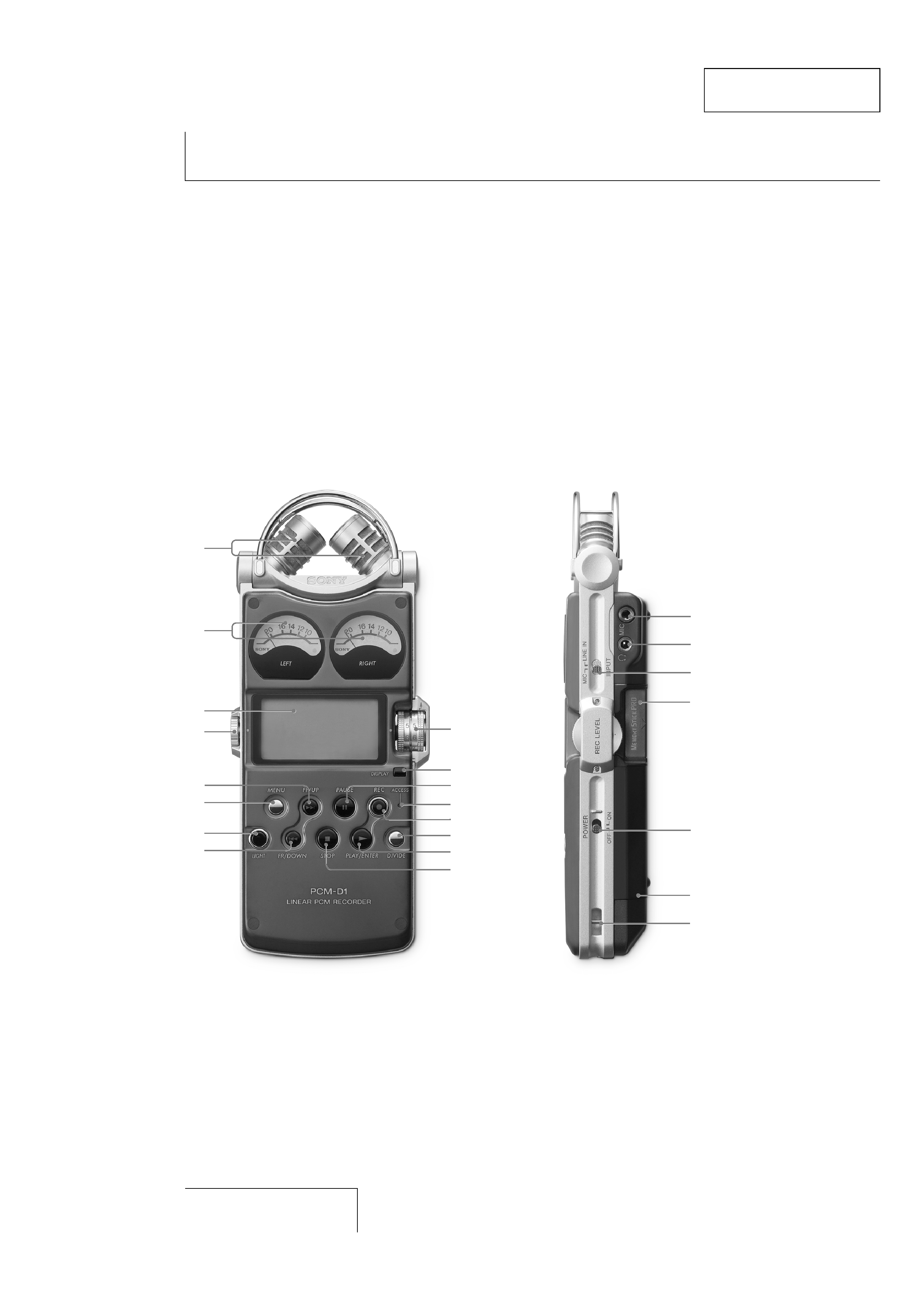
Identifying parts and controls
Front
Right side
1
Overview (continued)
2
3
4
5
6
8
7
9
0
qa
qs
qf
qg
qh
qd
qj
qk
ql
w;
wa
ws
wd
14
