-- 1 --
Model Name Using Similar Mechanism
MDS-JE500
MD Mechanism Type
MDM-3A
Optical Pick-up Type
KMS-260A/J1N
MDS-J3000/J3000ES
SERVICE MANUAL
AEP Model
UK Model
MDS-J3000ES
E Model
Chinese Model
MDS-J3000
MINIDISC DECK
MICROFILM
SPECIFICATIONS
-- Continued on next page --
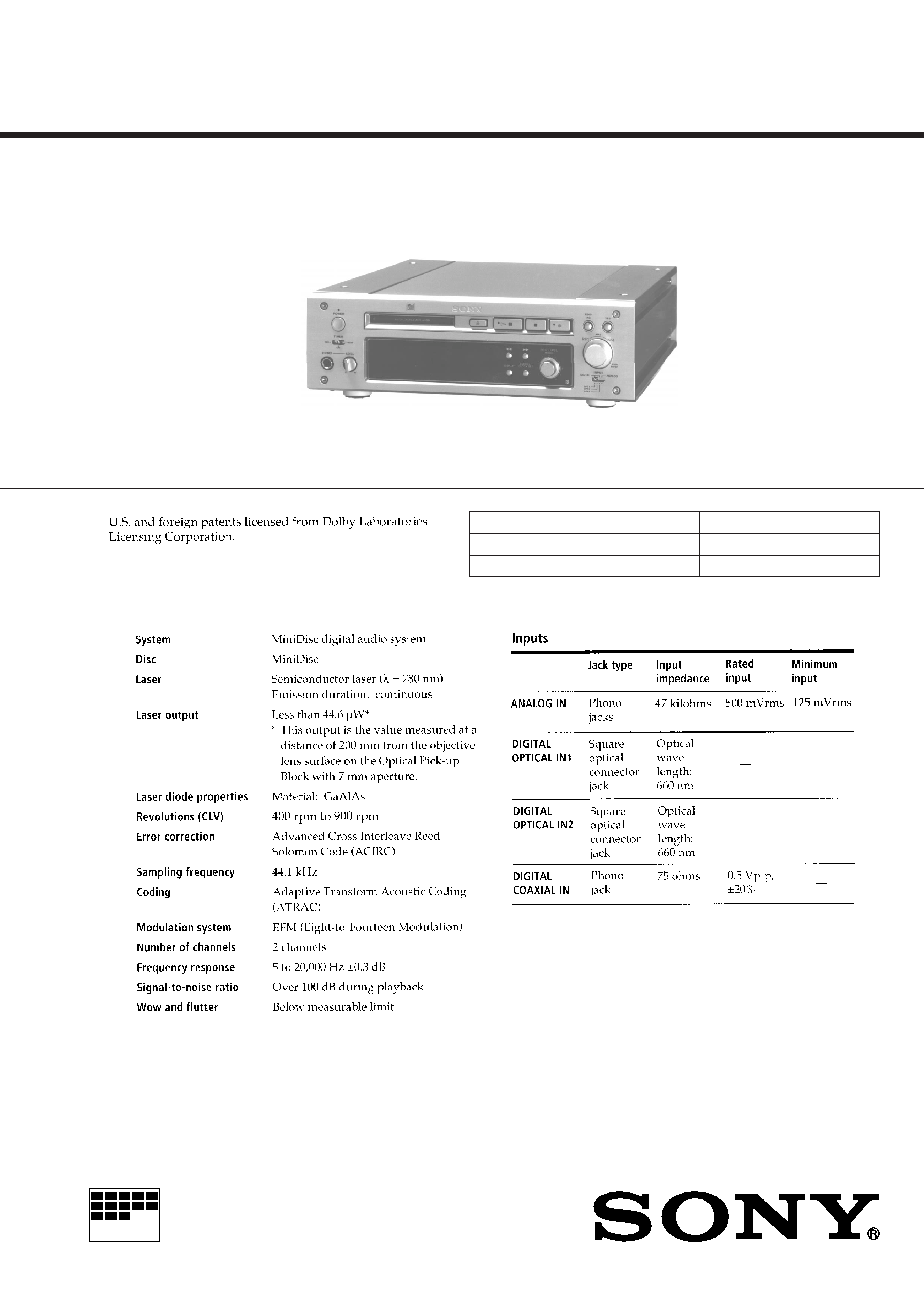
Photo: MDS-J3000

-- 2 --
CAUTION
Danger of explosion if battery is incorrectly replaced.
Replace only with the same or equivalent type recommended by
the equipment manufacturer.
Discard used batteries according to manufacture's instructions.
ADVARSEL!
Lithiumbatteri - Eksplosionsfare ved fejlagtig håndtering.
Udskiftning må kun ske med batteri af samme fabrikat og type.
Levér det brugte batteri tilbage til leverandøren.
ADVARSEL
Eksplosjonsfare ved feilakting skifte av batteri.
Benytt samme batteritype eller en tilsvarende type anbefalt av
apparatfabrikanten.
Brukte batterier katterier kasseres i henhold til fabrikantens
VARNIG
Explosionsfara vid felaktigt batteribyte.
Använd samma batterityp eller en likvärdig typ som rekommenderas
av apparattillverkaren.
Kassera använt batteri enligt gällande föreakrifter.
VAROITUS
Parist voi räjähtää, jos se on virheellisesti asennettu.
Vaihda paristo ainoastaan laitevalmistajan suosittelemaan tyyppiin.
Hävitä käytetty paristo valmistajan ohjeiden mukaisesti.
SAFETY-RELATED COMPONENT WARNING !!
COMPONENTS IDENTIFIED BY MARK
! OR DOTTED LINE
WITH MARK
! ON THE SCHEMATIC DIAGRAMS AND IN
THE PARTS LIST ARE CRITICAL TO SAFE OPERATION.
REPLACE THESE COMPONENTS WITH SONY PARTS
WHOSE PART NUMBERS APPEAR AS SHOWN IN THIS
MANUAL OR IN SUPPLEMENTS PUBLISHED BY SONY.
Notes on chip component replacement
· Never reuse a disconnected chip component.
· Notice that the minus side of a tantalum capacitor may be
damaged by heat.
Flexible Circuit Board Repairing
· Keep the temperature of soldering iron around 270°C
during repairing.
· Do not touch the soldering iron on the same conductor of the
circuit board (within 3 times).
· Be careful not to apply force on the conductor when soldering
or unsoldering.
This appliance is classified as a CLASS 1
LASER product. The CLASS 1 LASER
PRODUCT MARKING is located on the
rear exterior.
The following caution label is located
inside the unit.
CAUTION
Use of controls or adjustments or performance of procedures
other than those specified herein may result in hazardous ra-
diation exposure.
The laser component in this product is
capable of emitting radiation exceeding
the limit for Class 1.

-- 3 --
TABLE OF CONTENTS
1. SERVICING NOTE .......................................................... 4
2. GENERAL .......................................................................... 7
3. DISASSEMBLY
3-1. Front Panel Assembly ......................................................... 22
3-2. Bracket (T), (L) and (R) ...................................................... 22
3-3. BD Board ........................................................................... 23
3-4. SUB Chassis ........................................................................ 23
3-5. Shutter Assembly ................................................................ 24
3-6. Over Write Head ................................................................. 24
3-7. Slider Complete Assembly .................................................. 25
4. TEST MODE ..................................................................... 26
5. ELECTRICAL ADJUSTMENTS ............................... 29
6. DIAGRAMS
6-1. Circuit Boards Location ...................................................... 34
6-2. Block Diagrams
· BD Section ....................................................................... 35
· Main Section .................................................................... 37
6-3. IC Block Diagrams -- BD Section -- ................................ 39
6-4. Printed Wiring Board -- BD Section -- ............................. 42
6-5. Schematic Diagram -- BD Section -- ............................... 45
6-6. Schematic Diagram -- Main Section -- ............................ 49
6-7. Printed Wiring Board -- Main Section -- .......................... 53
6-8. Printed Wiring Board -- Panel Section -- ......................... 56
6-9. Schematic Diagram -- Panel Section -- ............................ 59
6-10. IC Block Diagrams -- Main Section -- .......................... 61
6-11. IC Pin Functions ............................................................... 63
7. EXPLODED VIEWS
7-1. Panel (Top, Rear, Side) Section .......................................... 72
7-2. Front Panel Section ............................................................. 73
7-3. Chassis Section .................................................................... 74
7-4. Mechanism Deck Section (1) (MDM-3A) .......................... 75
7-5. Mechanism Deck Section (2) (MDM-3A) .......................... 76
8. ELECTRICAL PARTS LIST ........................................ 77

-- 4 --
SECTION 1
SERVICING NOTE
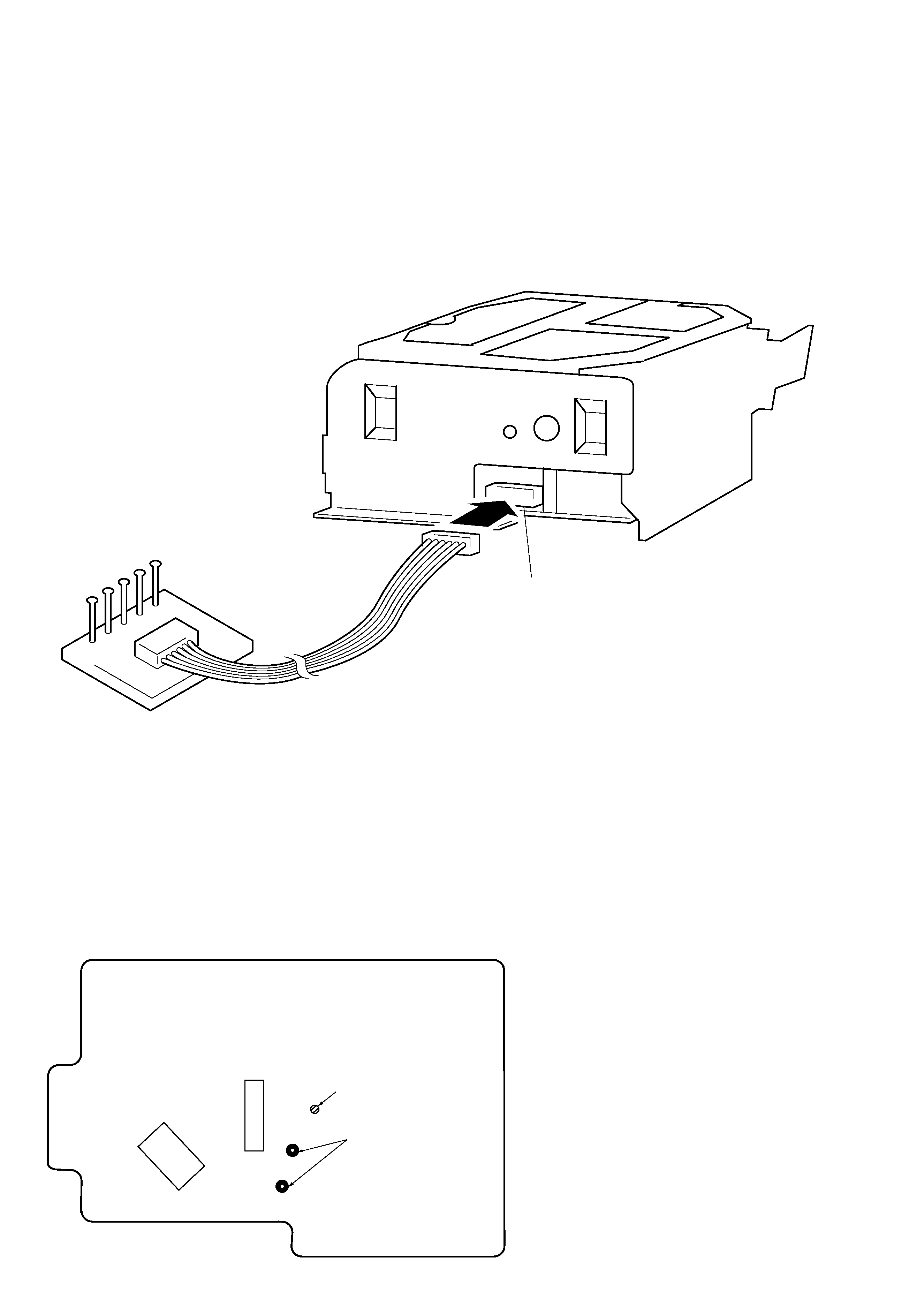
JIG FOR CHECKING BD BOARD WAVEFORM
The special jig (J-2501-124-A) is useful for checking the waveform of the BD board. The names of terminals and the checking items to be
performed are shown as follows.
I+3V : For measuring IOP (Check the deterioration of the optical pick-up laser)
IOP
: For measuring IOP (Check the deterioration of the optical pick-up laser)
TEO : TRK error signal (Traverse adjustment)
VC
: Reference level for checking the signal
RF
: RF signal (Check jitter)
IOP
I + 3V
TEO
VC
RF
Mechanism deck
CN110
Jig
(J-2501-124-A)
FORCED RESET
The system microprocessor can be reset in the following way.
Use these methods when the unit cannot be operated normally due to the overrunning of the microprocessor, etc.
Method :
Disconnect the power plug, short-circuit the land of RESET.
[MAIN BOARD] (Conductor Side)
Short land
TP (RESET)
CN303
IC401

-- 5 --
RETRY CAUSE DISPLAY MODE
· In this test mode, the causes for retry of the unit during recording can be displayed on the fluorescent display tube.
This is useful for locating the faulty part of the unit.
· The data amount stored in D RAM, number of retries, and retry cause are displayed. Each is displayed in hexadecimal number.
· The display of the D RAM data amount enables data reading, accumulation, ejection, and writing to be performed smoothly. If writing is
not smooth, data may decrease considerably.
Method:
1. Load a recordable disc whose contents can be erased into the unit.
2. Press the EDIT/NO button several times to display "All Erase?" on the fluorescent display tube.
3. Press the YES button.
4. When "All Erase??" is displayed on the fluorescent display tube, the numbers on the music calendar will start blinking.
5. Press the YES button to display "Complete", and press the
p button immediately and continue pressing for about 10 seconds.
6. When the "TOC" displayed on the fluorescent display tube goes off, release the
p button.
7. Press the
r REC button to start recording.
8. Press the DISPLAY button to display the test mode (Fig. 1), and check the display.
9. The Rt value increases with each retry. If an error occurs after a retry, "Retry Error" will be displayed, and the number of retries counted
will be set back to 0.
10. To exit the test mode, press the POWER button. Turn OFF the power, and after "TOC" disappears, disconnect the power plug from the
outlet.
Fig. 1 Reading the Test Mode Display
SC @@
Rt # #
Fluorescent Display Tube Signs
@@ : Displays the DRAM memory amount when at all times.
# #
: Displays the number of retries. When a retry error occurs, the number will be set back to 0.
* *
: Cause of retry
All three displays above are in hexadecimal numbers.
