ORDER NO.
PIONEER CORPORATION 4-1, Meguro 1-chome, Meguro-ku, Tokyo 153-8654, Japan
PIONEER ELECTRONICS SERVICE, INC. P.O. Box 1760, Long Beach, CA 90801-1760, U.S.A.
PIONEER ELECTRONIC (EUROPE) N.V. Haven 1087, Keetberglaan 1, 9120 Melsele, Belgium
PIONEER ELECTRONICS ASIACENTRE PTE. LTD. 253 Alexandra Road, #04-01, Singapore 159936
PIONEER CORPORATION 1999
RRV2194
DVD LD PLAYER
DVL-919 (1)
T ZZE AUG. 1999 Printed in Japan
Model No.
Order No.
Remarks
DVL-919/KU/CA
RRV2089
¶ This service manual should be used together with the following manual(s):
Type
Power Requirement
The voltage can be converted by
the following method.
Model
DVL-919 (1)
THIS MANUAL IS APPLICABLE TO THE FOLLOWING MODEL(S) AND TYPE(S).
Region No.
KU/CA2
AC120V
1
RD/RA2
AC110-127/220-240V
1
Automatic select
1. CONTRAST OF MISCELLANEOUS PARTS ........ 2
2. SCHEMATIC DIAGRAM ....................................... 4
3. PCB CONNECTION DIAGRAM ............................ 6
Confirm it ............................................................... 8
CONTENTS
DVL-919 has two models which specifications are different.
Each distinction will be confirmed with the indication of
the rear cover and the packing case.
Refer to " Confirm it ".

DVL-919 (1)
2
1. CONTRAST OF MISCELLANEOUS PARTS
7 CONTRAST TABLE FOR KU/CA2 TYPE
KU/CA2 type and KU/CA type are constructed the same except for the following:
ASSEMBLIES
P7 8
DVDM ASSY
VWS1377
VWS1397
BOTTOM VIEW SECTION
P929
REAR COVER
VNA2028
VNA2144
Ref.
No.
Remarks
KU/CA type
KU/CA2 type
Part No.
Mark
Symbol and Description
NOTES :
÷ Parts marked by " NSP " are generally unavailable because they are not in our Master Spare Parts List.
÷ The
mark found on some component parts indicates the importance of the safety factor of the part.
Therefore, when replacing, be sure to use parts of identical designation.
÷ Reference Nos. indicate the pages and Nos. in the service manual for the base model.
÷ When ordering resistors, first convert resistance values into code form as shown in the following examples.
Ex. 1
When there are 2 effective digits (any digit apart from 0), such as 560 ohm and 47k ohm (tolerance is shown by
J = 5%, and K = 10%).
560
= 56 × 101= 561 ................................................... RD1/4PU 5 6 1 J
47k
= 47 × 10 3 = 473 .................................................. RD1/4PU 4 7 3 J
0.5
= R50 ...................................................................... RN2H Â 5 0 K
1
= 1R0 ......................................................................... RS1P 1 Â 0 K
Ex. 2
When there are 3 effective digits (such as in high precision metal film resistors).
5.62k
= 562 × 10 1 = 5621 ........................................... RN1/4PC 5 6 2 1 F
¶ For PCB ASSEMBLIES, Refer to "CONTRAST OF PCB ASSEMBLIES", "2. SCHEMATIC DIAGRAM" and "3. PCB CONNECTION DIAGRAM".
7 CONTRAST TABLE FOR RD/RA2 TYPE
RD/RA2 type and RD/RA type are constructed the same except for the following:
ASSEMBLIES
P7 8
DVDM ASSY
VWS1377
VWS1397
BOTTOM VIEW SECTION
LABEL
Not used
VRW1789
No. 1
Ref.
No.
Remarks
RD/RA type
RD/RA2 type
Part No.
Mark
Symbol and Description
¶ The numbers in the remarks column correspond to the numbers on the "EXPLODED VIEWS".
¶ For PCB ASSEMBLIES, Refer to "CONTRAST OF PCB ASSEMBLIES", "2. SCHEMATIC DIAGRAM" and "3. PCB CONNECTION DIAGRAM".

DVL-919 (1)
3
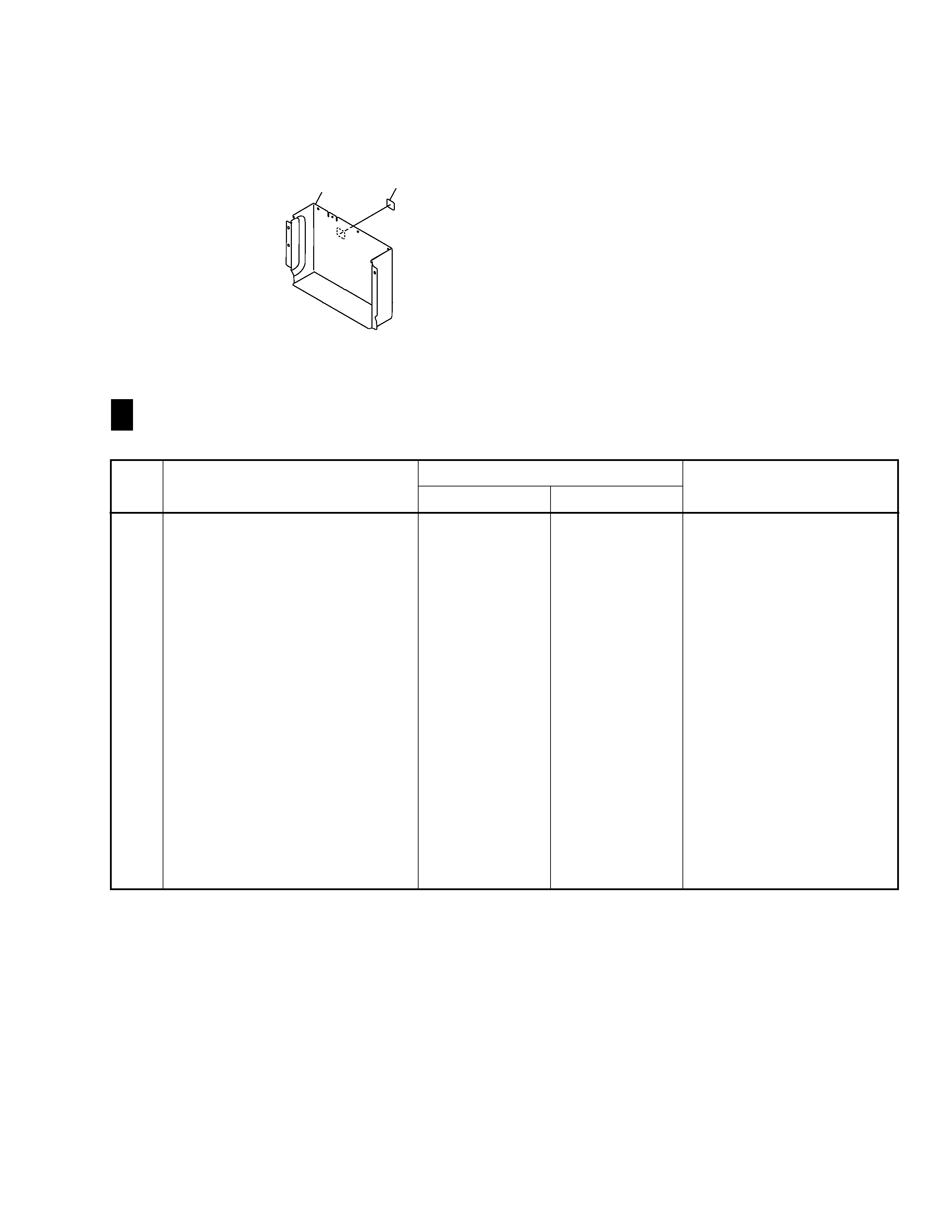
7 EXPLODED VIEWS
÷ EXTERIOR
No. 1
Rear Cover
IC451
Not used
PQ2TZ15
IC603
VYW1639
VYW1657
IC801
MB86371C
MB86373
C451
Not used
CKSQYF105Z16
C813, C814, C826
CEV101M6R3
CEV221M4
C899 (2.2
µF)
Not used
VCG1031
R801
RS1/16S272J
RS1/16S2401F
R816
RS1/16S102J
RS1/16S2701F
R817
Not used
RS1/16S2701F
R818
Not used
RS1/16S103J
R820
RS1/16S681J
RS1/16S1201F
R823 -R825
RS1/16S1500F
Not used
R834, R854, R874
RS1/16S1201F
Not used
R840, R860, R882
Not used
RS1/16S1201F
R843, R863, R878
Not used
RS1/16S1600F
R893
RS1/10S0R0J
Not used
R3866, R3877, R3886
Not used
RS1/16S0R0J
VR801 (1k
)
VCP1125
Not used
Mark
Symbol and Description
Part No.
VWS1377
VWS1397
Remarks
DVDM ASSY
VWS1397 and VWS1377 are constructed the same except for the following:
7 CONTRAST TABLE OF PCB ASSEMBLIES
F
I

DVL-919 (1)
4
A
B
C
D
1
23
4
12
3
4
I
(VWS1397)
DVDM ASSY
I 3/3 F
I 2/3
I 2/3
I 2/3
I 2/3
I 2/3
2/3
I
I
2/3
I 2/3
I 2/3
I 2/3 I 1/3
J
2/3
CN201
I 1/3
I 2/3
I 2/3
STANDBY
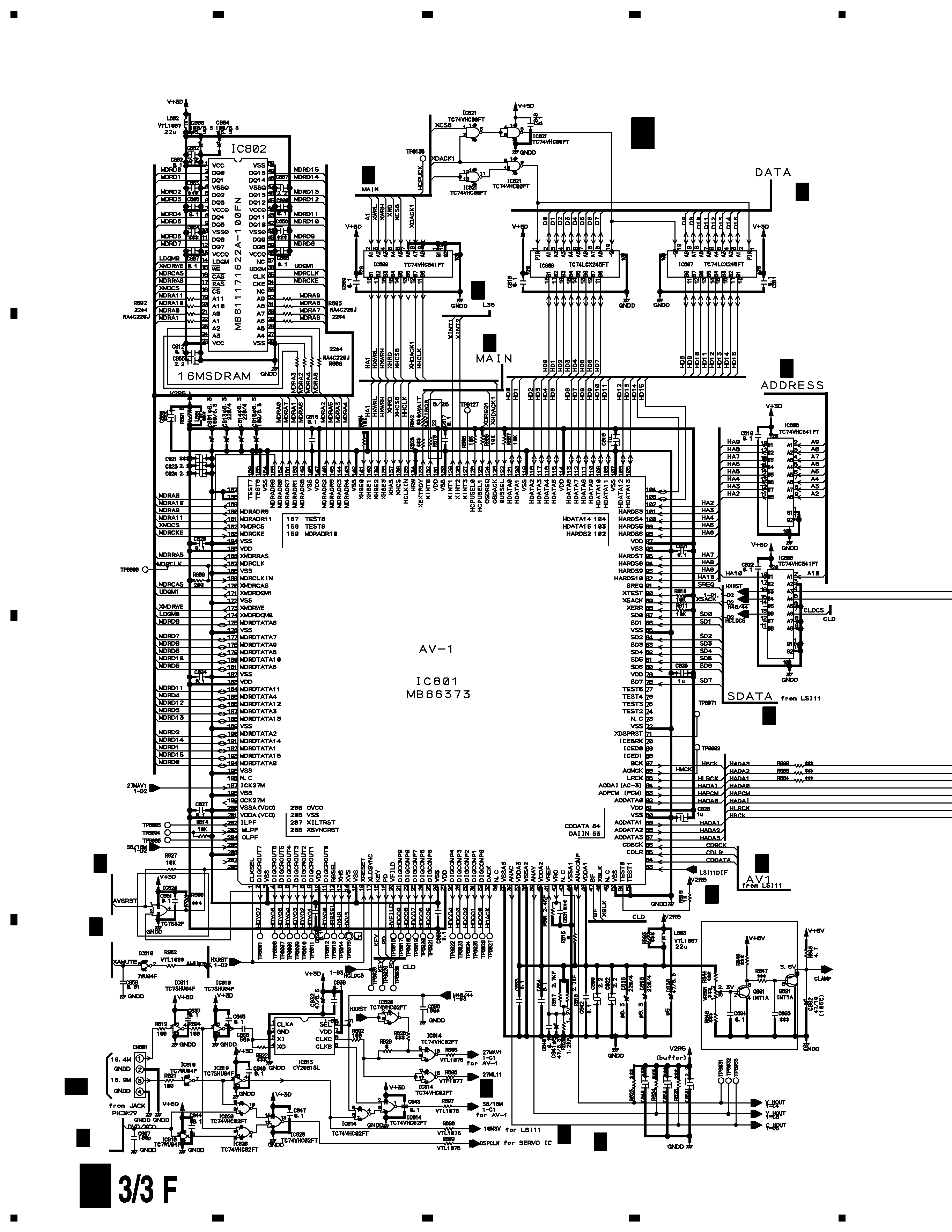
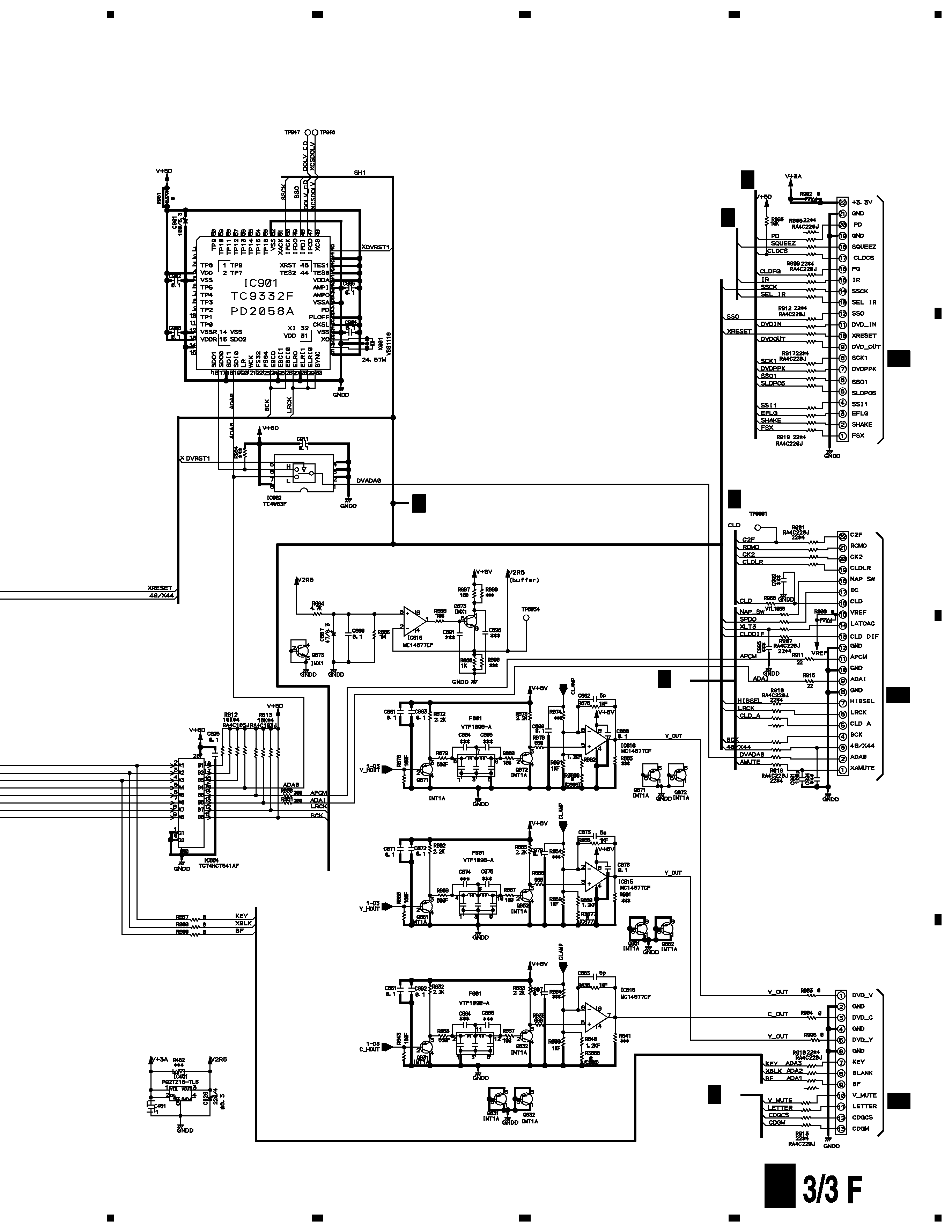
2. SCHEMATIC DIAGRAM
2.1 DVDM ASSY (3/3)

DVL-919 (1)
5
A
B
C
D
5
67
8
5
6
7
8
I
HIBSEL,48/X44,XRESET,XLT3
I 2/3
I 2/3
I 1/3
I 1/3
I 2/3
I 2/3
J
1/3
CN111
J
2/3
CN122
K
2/2
CN601
CN902
VKN1426
CN901
VKN1426
CN903
S13B-PH-SMB
Note : When ordering service parts, be sure to refer to "EXPLODED VIEWS and PARTS LIST" or "PCB PARTS LIST".
