ORDER NO.
PIONEER CORPORATION 4-1, Meguro 1-chome, Meguro-ku, Tokyo 153-8654, Japan
PIONEER ELECTRONICS SERVICE, INC. P.O. Box 1760, Long Beach, CA 90801-1760, U.S.A.
PIONEER EUROPE NV Haven 1087, Keetberglaan 1, 9120 Melsele, Belgium
PIONEER ELECTRONICS ASIACENTRE PTE. LTD. 253 Alexandra Road, #04-01, Singapore 159936
PIONEER CORPORATION 2000
RRV2307
DVD PLAYER
T ZZE JUNE 2000 Printed in Japan
Model No.
Order No.
Remarks
DV-333/KUXJ
RRV2290
¶ This service manual should be used together with the following manual(s):
DV-434
Type
Power Requirement
Remarks
Model
DV-434
THIS MANUAL IS APPLICABLE TO THE FOLLOWING MODEL(S) AND TYPE(S).
Region No.
KUXJ
AC120V
1
KCXJ
AC120V
1
DV-434
2
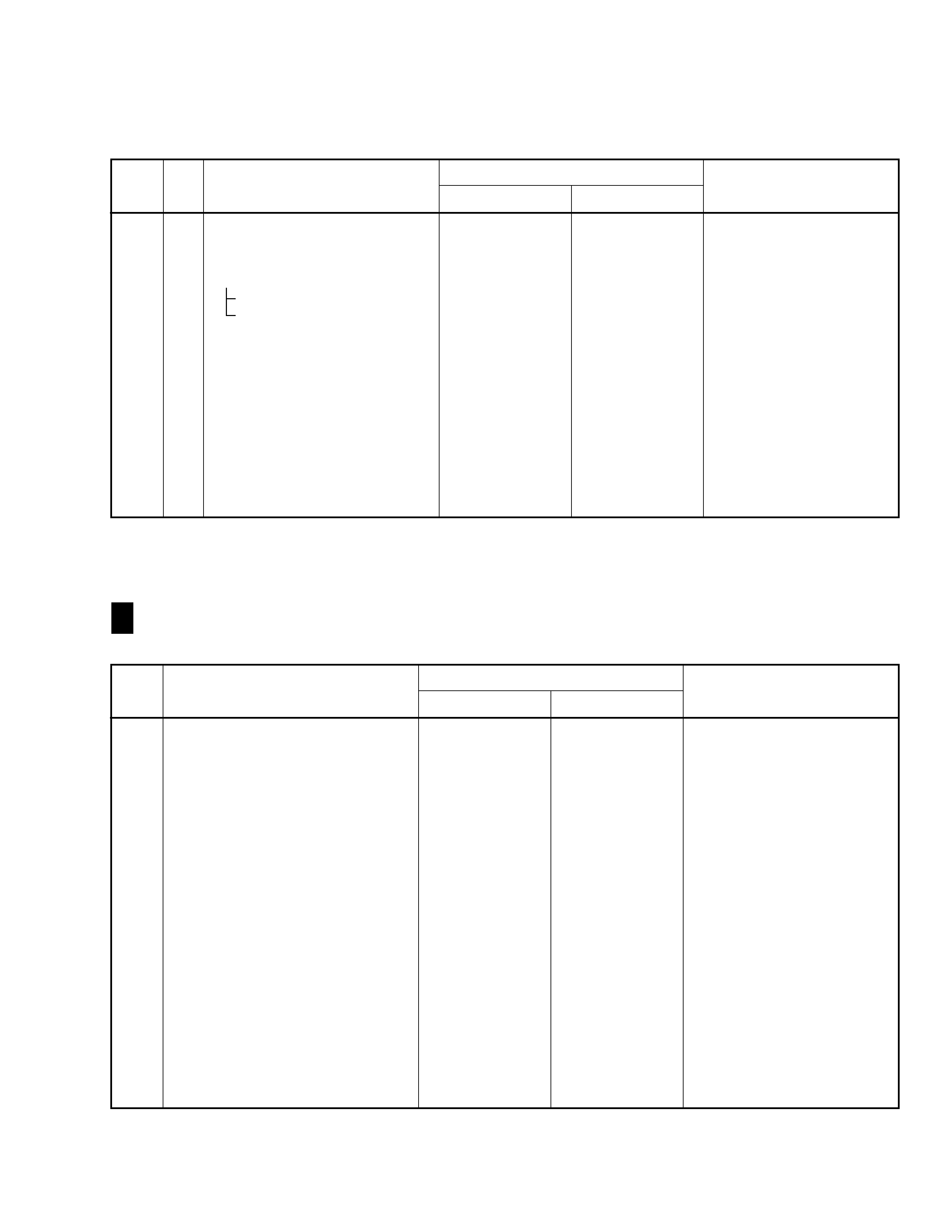
7 CONTRAST TABLE for DV-434/KUXJ
DV-434/KUXJ and DV-333/KUXJ are constructed the same except for the following:
PCB ASSEMBLIES
P5 - 1
DVDM Assy
VWS1412
VWS1432
FLJB Assy
VWM1991
VWM2049
P5 - 4
FLJB Assy
VWV1748
VWV1780
P5 - 2
NSP
PWSB Assy
VWG2174
VWG2243
PACKING
P3 - 4
Remote Control Unit
VXX2702
VXX2703
P3 - 9
Packing Case
VHG1901
VHG1924
P3 -13
Operating Instructions (English)
VRB1244
VRB1252
EXTERIOR
P5 -12
Rear Panel
VNA2161
VNA2183
P5 -17
Front Panel Assy
VXA2391
VXA2399
P5 -19
NSP
Pop Label
VRW1830
VRW1833
NSP
Pop Label
Not used
VRW1845
For Front Panel
Ref.
No.
Remarks
DV-333/KUXJ
DV-434/KUXJ
Part No.
Mark
Symbol and Description
1. CONTRAST OF MISCELLANEOUS PARTS
· For PCB assemblies, Refer to "CONTRAST OF PCB ASSEMBLIES" and "2. SCHEMATIC DIAGRAM".
NOTES :
÷ Parts marked by " NSP " are generally unavailable because they are not in our Master Spare Parts List.
÷ The
mark found on some component parts indicates the importance of the safety factor of the part.
Therefore, when replacing, be sure to use parts of identical designation.
÷ Reference Nos. indicate the pages and Nos. in the service manual for the base model.
÷ When ordering resistors, first convert resistance values into code form as shown in the following examples.
Ex. 1
When there are 2 effective digits (any digit apart from 0), such as 560 ohm and 47k ohm (tolerance is shown by
J = 5%, and K = 10%).
560
= 56 × 101= 561 ................................................... RD1/4PU 5 6 1 J
47k
= 47 × 10 3 = 473 .................................................. RD1/4PU 4 7 3 J
0.5
= R50 ...................................................................... RN2H Â 5 0 K
1
= 1R0 ......................................................................... RS1P 1 Â 0 K
Ex. 2
When there are 3 effective digits (such as in high precision metal film resistors).
5.62k
= 562 × 10 1 = 5621 ........................................... RN1/4PC 5 6 2 1 F
DV-434
3
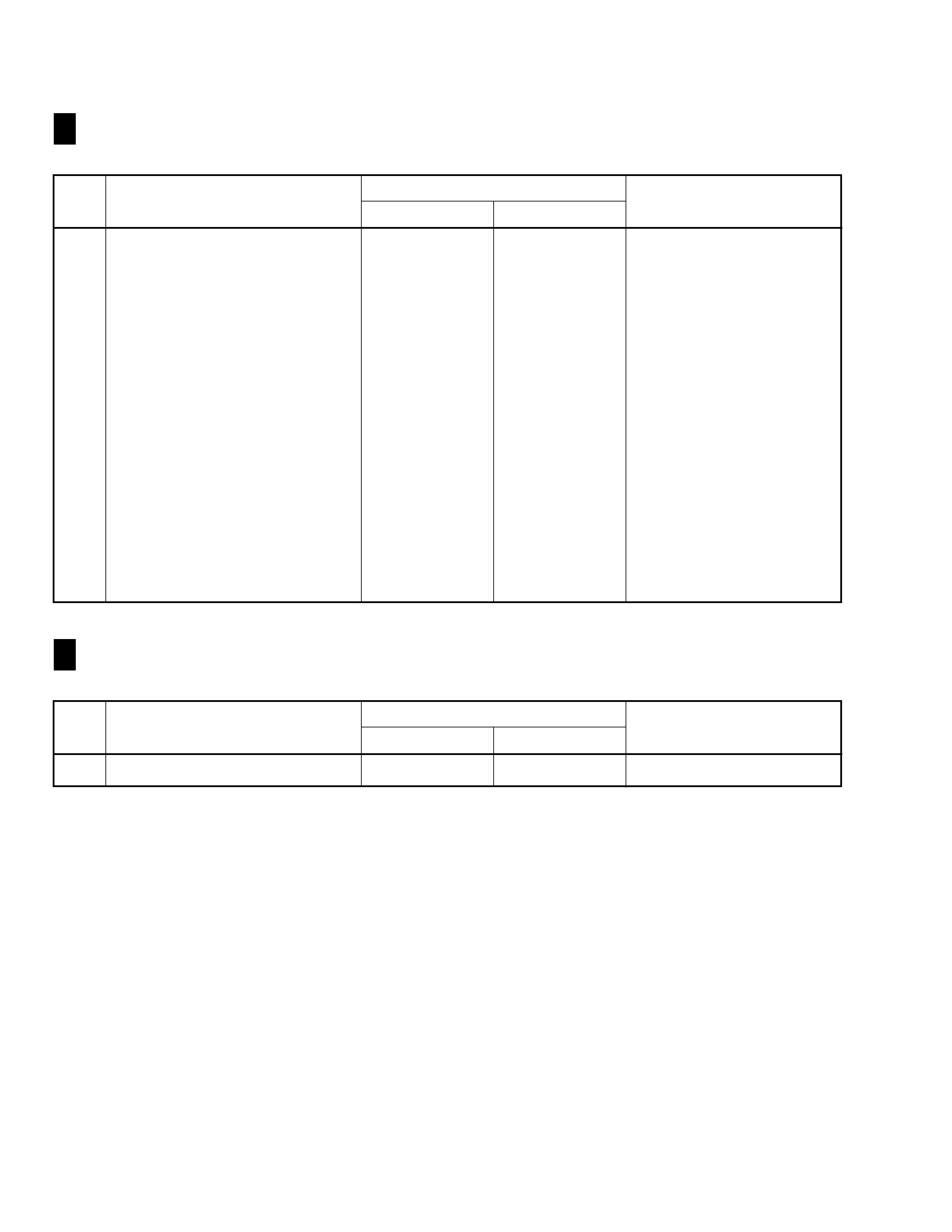
7 CONTRAST TABLE for DV-434/KCXJ
DV-434/KCXJ and DV-333/KCXJ are constructed the same except for the following:
PCB ASSEMBLIES
P5 - 1
DVDM Assy
VWS1412
VWS1432
FLJB Assy
VWM1991
VWM2049
P5 - 4
FLJB Assy
VWV1748
VWV1780
P5 - 2
NSP
PWSB Assy
VWG2174
VWG2243
PACKING
P3 - 4
Remote Control Unit
VXX2702
VXX2703
P3 - 9
Packing Case
VHG1923
VHG1950
P3 -13
Operating Instructions (English)
VRB1244
VRB1252
P3 -14
Operating Instructions (French)
VRC1116
VRC1115
EXTERIOR
P5 -12
Rear Panel
VNA2161
VNA2183
P5 -17
Front Panel Assy
VXA2391
VXA2399
P5 -19
NSP
Pop Label
VRW1830
Not used
Ref.
No.
Remarks
DV-333/KCXJ
DV-434/KCXJ
Part No.
Mark
Symbol and Description
· For PCB assemblies, Refer to "CONTRAST OF PCB ASSEMBLIES" and "2. SCHEMATIC DIAGRAM".
7 CONTRAST OF PCB ASSEMBLIES
IC27
Not used
PM0026A
Q87, Q89, Q91
Not used
2SA1576A
C834C836, C865C869, C871876
Not used
CKSRYF104Z16
C861C864
Not used
CKSRYF105Z16
C870
Not used
CKSQYB104Z25
R1
Not used
RS1/16S103J
For CHECKER
R2
RS1/16S103J
Not used
For CHECKER
R866
Not used
RS1/16S103J
R501, R502
RS1/16S0R0J
Not used
R808
Not used
RS1/16S8202F
R822R824
Not used
RS1/16S1200F
R845R847
Not used
RS1/16S182J
R854, R856
Not used
RS1/16S4R7J
R855, R861R865, R868R871
Not used
RS1/16S0R0J
R971R974, R8640
Not used
RS1/16S0R0J
R872
Not used
RS1/16S3001F
R873
Not used
RS1/16S6800F
R874
Not used
RS1/16S1201F
R8610, R8620, R8630
Not used
RS1/10S0R0J
Mark
Symbol and Description
Part No.
VWS1412
VWS1432
Remarks
DVDM ASSY
VWS1432 and VWS1412 are constructed the same except for the following:
F
D
DV-434
4
IC501
Not used
TC74HC4053AF
Q500
Not used
DTC114YK
Q531, Q541, Q551
Not used
2SA1037K
D101
Not used
SLR-56VC
F501F503
12MHz LPF(VIDEO)
Not used
VTF1158
C451
CEAT471M6R3
CEAT102M6R3
C530, C540
Not used
CKSRYF104Z25
C531, C541, C551
Not used
CCSQCH6R0D50
R140
RS1/10S0R0J
RS1/10S622J
R142
Not used
RS1/10S363J
R160, R533, R543, R553, R594
Not used
RS1/10S0R0J
R163
Not used
RS1/10S181J
R407, R408, R505, R515
RS1/10S0R0J
Not used
R458, R462
RS1/10S3300D
RS1/10S3900D
R500
Not used
RS1/10S472J
R531, R541, R551
Not used
RS1/10S3300D
R532, R542, R552
Not used
RS1/10S2202D
R534, R544, R554
Not used
RS1/10S182J
Mark
Symbol and Description
Part No.
VWV1748
VWV1780
Remarks
FLJB ASSY
VWV1780 and VWV1748 are constructed the same except for the following:
S801
Not used
ASG7013
Mark
Symbol and Description
Part No.
VWG2174
VWG2243
Remarks
PWSB ASSY
VWG2243 and VWG2174 are constructed the same except for the following:
F
E
F
G

DV-434
5