ORDER NO.
PIONEER CORPORATION 4-1, Meguro 1-chome, Meguro-ku, Tokyo 153-8654, Japan
PIONEER ELECTRONICS (USA) INC. P.O. Box 1760, Long Beach, CA 90801-1760, U.S.A.
PIONEER EUROPE NV Haven 1087, Keetberglaan 1, 9120 Melsele, Belgium
PIONEER ELECTRONICS ASIACENTRE PTE. LTD. 253 Alexandra Road, #04-01, Singapore 159936
PIONEER CORPORATION 2005
RRV3107
T ZZY FEB. 2005 Printed in Japan
¶ This service manual should be used together with the following manual(s):
Model No.
Order No.
Remarks
DJM-500/RELM
RRV1405
THIS MANUAL IS APPLICABLE TO THE FOLLOWING MODEL(S) AND TYPE(S).
Model
DJM-500
Type
Power Requirement
The voltage can be converted by the
following method.
RELM4
DJM-500
AC110-120V/220-240V
DJ MIXER
With the voltage selector
2
A
B
C
D
1
23
4
12
3
4
DJM-500
1. CONTRAST OF MISCELLANEOUS PARTS
Parts marked by "NSP" are generally unavailable because they are not in our Master Spare Parts List.
The
mark found on some component parts indicates the importance of the safety factor of the part.
Therefore, when replacing, be sure to use parts of identical designation.
Screws adjacent to
mark on product are used for disassembly.
Reference Nos. indicate the pages and Nos. in the service manual for the base model.
NOTES:
When ordering resistors, first convert resistance values into code form as shown in the following examples.
Ex.1 When there are 2 effective digits (any digit apart from 0), such as 560 ohm and 47k ohm (tolerance is shown by J=5%,
and K=10%).
Ex.2 When there are 3 effective digits (such as in high precision metal film resistors).
561
473
R50
1R0
5621
560
47k
0.5
1
RD1/4PU
J
RD1/4PU
J
RN2H
K
RS1P
K
56
x 101
47
x 103
R50
1R0
561
473
5.62k
RN1/4PC
F
562
x 101
5621
DJM-500/RELM4 and DJM-500/RELM are constructed the same except for the following :
PCB ASSEMBLIES
NSP
DSP ASSY
DWX1786
DWX2464
P 4 - 8
TERMINAL ASSY
DWZ1076
DWZ1148
NSP
VR Assy
DWM2057
DWM2210
P4 - 10
NSP
PHONE JACK ASSY
DWZ1057
DWZ1144
P4 - 11
NSP
MIC JACK ASSY
DWZ1066
DWZ1145
NSP
SUB Assy
DWM2058
DWM2211
P4 - 20
NSP
BAL.OUT ASSY
DWZ1059
DWZ1147
P4 - 21
PHONE ASSY
DWZ1077
DWZ1146
PACKING
P3 - 8
Polyethylene Bag (0.03 x 230 x 340)
Z21-038
Not used
P3 - 8
Polyethylene Bag (0.06 x 230 x 340)
Not used
AHG7117
IEC 65-6 Caution
Not used
ARM7067
For Accessories
EXTERIOR
P4 - 35
Label
DRW1739
DRW2268
P4 - 57
Display Panel A
DAH2095
DAH2177
P4 - 59
Display Panel B
DAH2096
DAH2178
P4 - 116
NSP
Cord Clamper
RNE-513
Not used
CONTRAST TABLE
Part No.
DJM-500/
RELM
Ref. No.
Symbol and Description
Remarks
Mark
DJM-500/
RELM4
· For PCB ASSEMBLIES, Refer to " CONTRAST OF PCB ASSEMBLIES ".
3
A
B
C
D
5
67
8
5
6
7
8
DJM-500
CONTRAST OF PCB ASSEMBLIES
· MIC JACK Assy
DWZ1066 and DWZ1145 are constructed the same except for the following :
Mark
Symbol and Description
Part No.
DWZ1066
DWZ1145
Remarks
C1005
Not used
CCSRCH221J50
*3
*3 : Refer to " 2. SCHEMATIC DIAGRAM and 3. PCB CONNECTION DIAGRAM".
· PHONE JACK Assy
DWZ1057 and DWZ1144 are constructed the same except for the following :
Mark
Symbol and Description
Part No.
Remarks
DWZ1057
DWZ1144
C1003, C1004
Not used
CKSRYB104K25
*2
· PHONE Assy
DWZ1077 and DWZ1146 are constructed the same except for the following :
Mark
Symbol and Description
Part No.
Remarks
DWZ1077
DWZ1146
C602, C621, C622, C646
CCCSL101J50
CQMA102J50
C1101 - C1104
Not used
CCPUSL470J50
*4
C1105 - C1110
Not used
CCPUSL560J50
*4
· TERMINAL Assy
DWZ1076 and DWZ1148 are constructed the same except for the following :
Mark
Symbol and Description
Part No.
Remarks
DWZ1076
DWZ1148
R878 - R883
RD1/4PU101J
RD1/4PU332J
C867, C869, C875, C877, C879, C881
CCCSL101J50
Not used
C868, C870, C876, C878, C880, C882
CCCSL101J50
CQMA221J50
L901 - L906
Not used
LAU221J
*1
*1 : Refer to " 2. SCHEMATIC DIAGRAM and 3. PCB CONNECTION DIAGRAM".
*4 : Refer to " 2. SCHEMATIC DIAGRAM and 3. PCB CONNECTION DIAGRAM".
· BAL.OUT Assy
Although DWZ1059 and DWZ1147 are different in part number, they consist of the same components.
*2 : Refer to " 2. SCHEMATIC DIAGRAM and 3. PCB CONNECTION DIAGRAM".
4
A
B
C
D
1
23
4
12
3
4
DJM-500
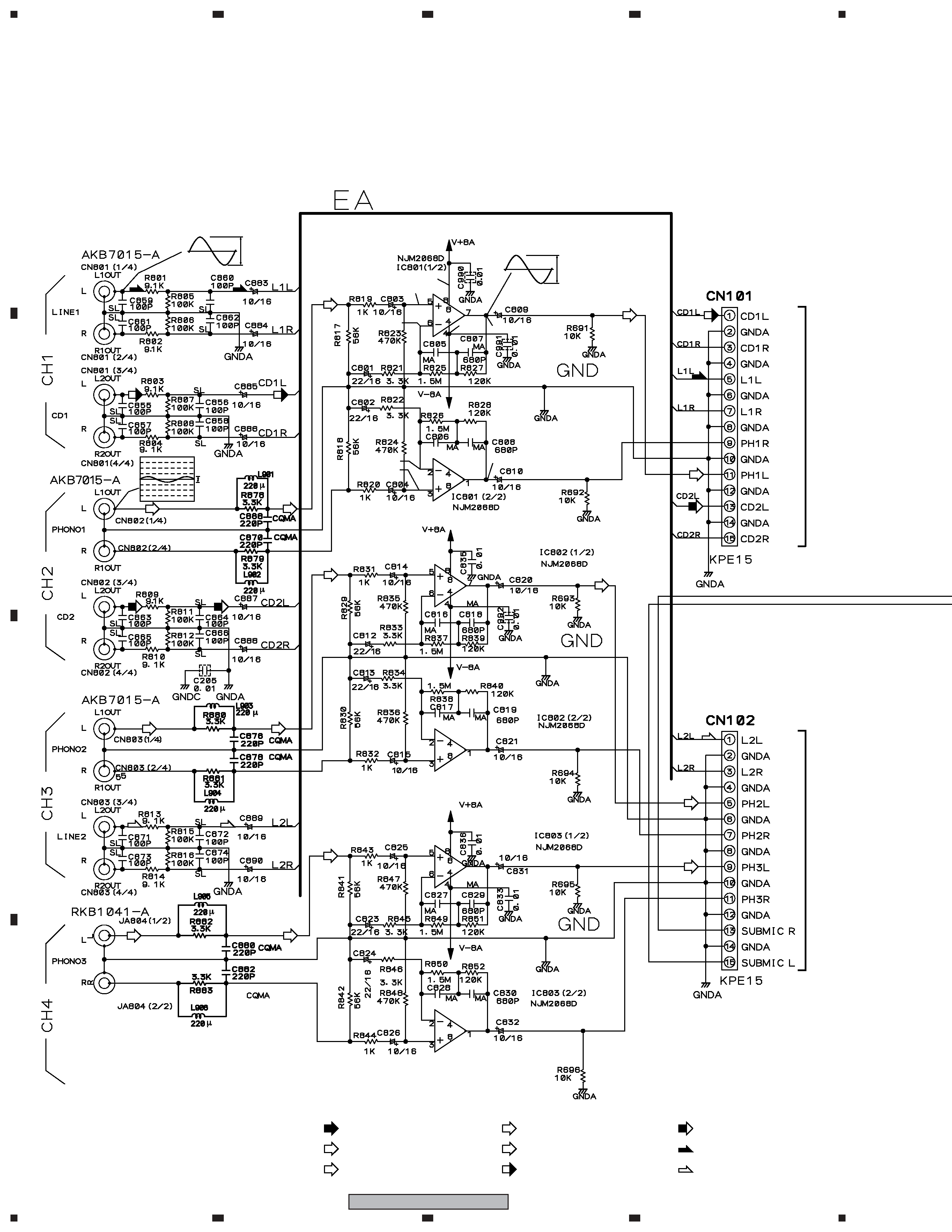
2. SCHEMATIC DIAGRAM
2.1 TERMINAL ASSY
To
INPUT
ASSY
(J101)
To
INPUT
ASSY
(J102)
: AUDIO SIGNAL
: RETURN SIGNAL
: PHONO1 (CH2) SIGNAL
: PHONO2 (CH3) SIGNAL
: PHONO3 (CH4) SIGNAL
: CD (CH1) SIGNAL
: CD (CH2) SIGNAL
: LINE1 (CH1) SIGNAL
: LINE2 (CH3) SIGNAL
(R)
(P1)
(P2)
(P3)
(P1)
0.1V/div 0.2ms/div
-14dB,1KHz
0.56Vp-p
GND
10mVp-p
20mV/div 0.2ms/div
-54dB,1KHz
(P1)
(P1)
(P2)
(P2)
(P2)
(P2)
(P3)
(P3)
(P3)
(P3)
(P2)
(P1)
(P1)
50mV/div 0.2ms/div
1KHz
260mVp-p
8.04
-7.95
106.3mV
247.3mV
106.7mV
104.7mV
-252.3mV
104.9mV
TERMINAL ASSY (DWZ1148)
5
A
B
C
D
5
67
8
5
6
7
8
DJM-500
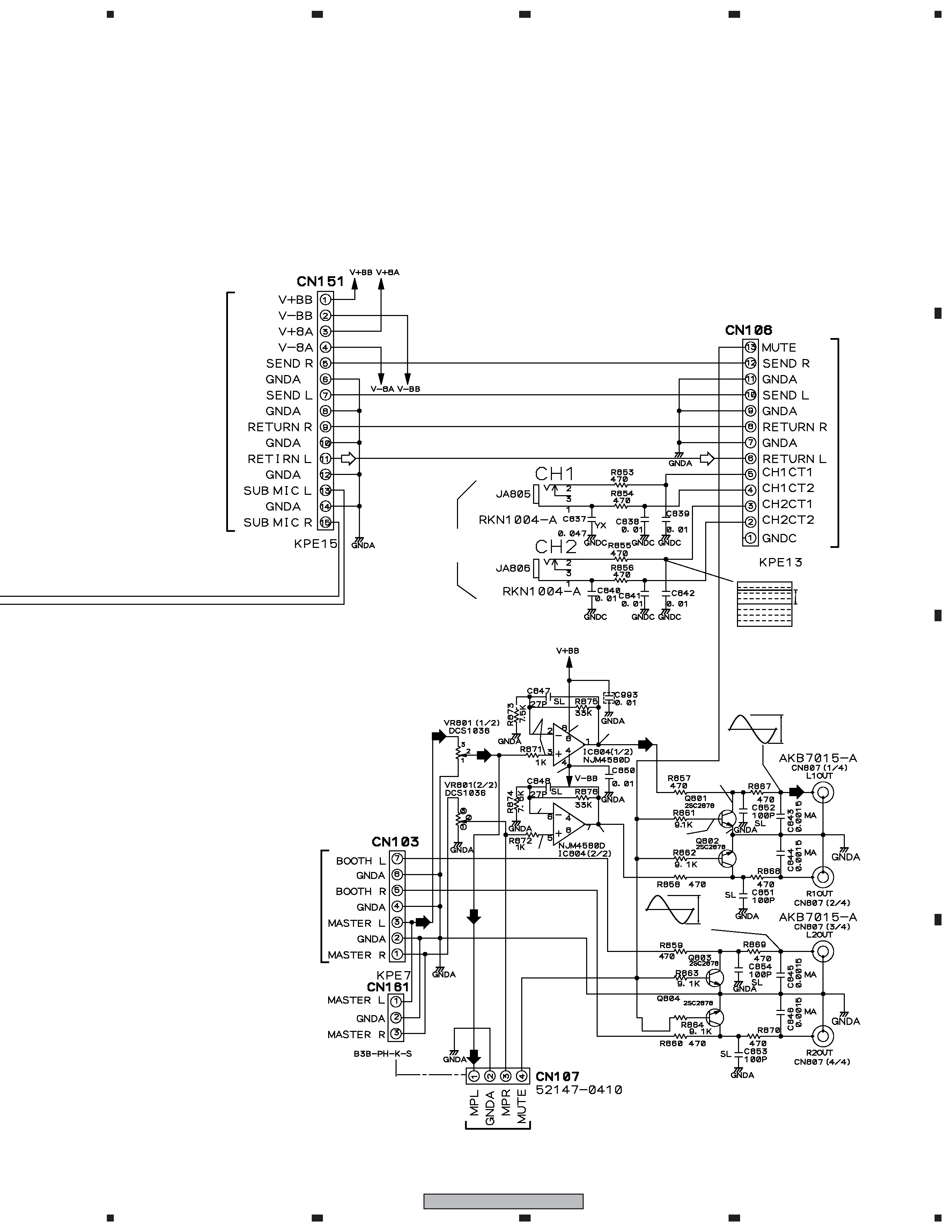
To
VR
ASSY
(J103)
To
PHONE
ASSY
(J151)
To PHONE ASSY (CN107)
To
DSP
ASSY
(J106)
PLAYER
CONTROL
(R)
(R)
GND
5Vp-p
2V/div
3.6mV
15.19
14.1mV
-15.33
3.9mV
3.9mV
15.8mV
14.4mV
-563mV
0
0.5V/div 20ms/div
1KHz
2.6Vp-p
0.5V/div 0.2ms/div
1KHz
1.6Vp-p
