PIONEER ELECTRONIC CORPORATION
4-1, Meguro 1-Chome, Meguro-ku, Tokyo 153-8654, Japan
PIONEER ELECTRONICS SERVICE INC.
P.O.Box 1760, Long Beach, CA 90801-1760 U.S.A.
PIONEER ELECTRONIC [EUROPE] N.V.
Haven 1087 Keetberglaan 1, 9120 Melsele, Belgium
PIONEER ELECTRONICS ASIACENTRE PTE.LTD. 501 Orchard Road, #10-00, Wheelock Place, Singapore 238880
C PIONEER ELECTRONIC CORPORATION 1998
K-ZZB. OCT. 1998 Printed in Japan
ORDER NO.
CRT2291
MD MECHANISM MODULE
CX-893
Service
Manual
CONTENTS
1. CIRCUIT DESCRIPTIONS...........................................2
2. DISASSEMBLY.........................................................13
- This service manual outlines operations of the MD mechanism module used in the models listed
below.
- For repair, use this Service Manual and the Service Manual of the model used in the system.
Model
Service manual
MD mechanism module
MEH-P5000R/EW
CRT2287
CXB2784

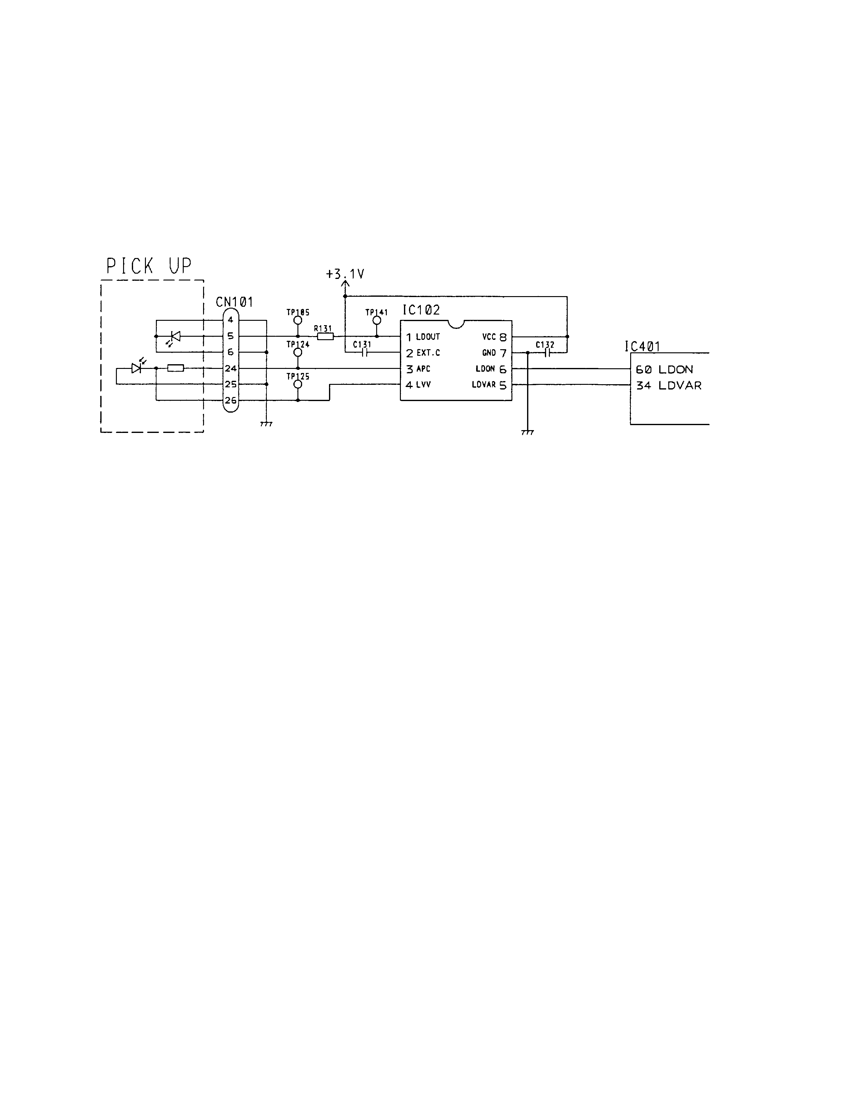
Figure 1 below shows the block diagram. This block
controls the output from the block LD to be consistent
with the monitor diode.
The block consists of IC 102 and turned to LD ON when
LDON (6 pin) is H and to LD OFF when LDON is L. LD
output level is set with the voltage value of LDVAR and
is usually around 2.4 V.
2
CX-893
1. CIRCUIT DESCRIPTION
1.1 APC Part
Fig.1
1.2 RF amplifying part
The block amplifies the pickup output signal and
generates RF and ADIP signals.
This block mainly consists of IC101.
REFO part
REFO (+1.5 V) is the reference voltage for the servo.
The signal is resistive divided at the IC (REFI: 5 pin) and
output to 6 pin through buffer. This signal will be the
reference for RFIC.
RF signal amplifying part
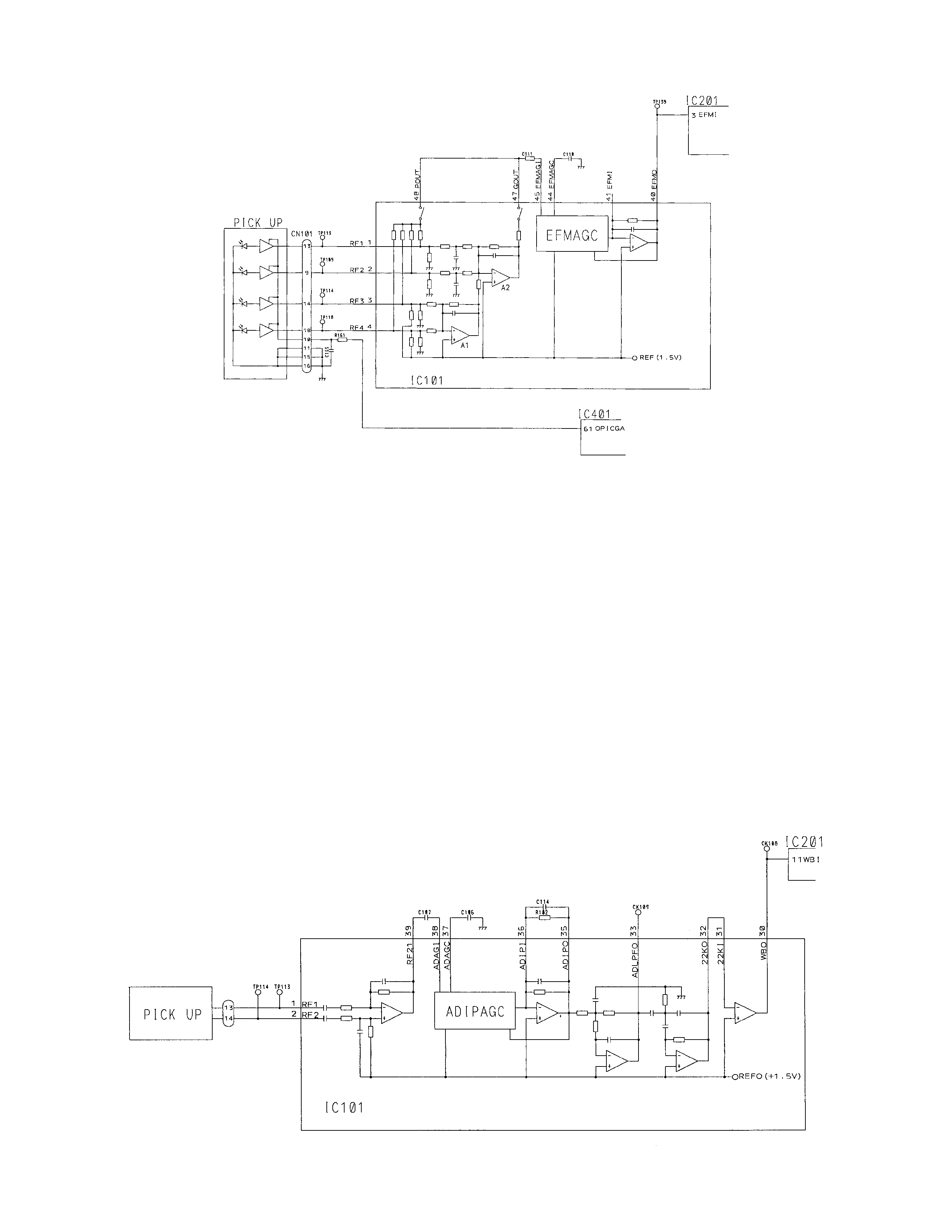
Figure 2 below shows the block diagram. The signal
which is I-V converted at the pickup is input to the RF1-4
(1-4 pin). Gain at the I-V amplifier contained in the PU
is switched depending on the disc types. The switching
is controlled by OPICGA (IC401, 61 pin) and H is output
at Premaster DISC and L is output at Recordable DISC.
The signal input from the I-V amplifier is operated with
the contained resistance and amplifiers (A1, A2) and the
signal (RF1 + RF2 + RF3 + RF4) (POUT) and the signal
(RF1 + RF2 + RF3 - RF4) (GOUT) are generated. Each of
POUT and GOUT is equipped with an analog switch.
The switches are controlled with the DISC signal (bits
on microprocessor serial communications). The POUT
signal is output through 48 pin when the DISC signal is
H (PIT mode) and GOUT signal is output through 47 pin
when the DISC signal is L (GRV mode).
These signals are input to EFMAGC (45 pin) through the
coupling capacitors (C133, C112) and transmitted to the
AGC circuit and filter part to be output from EFMO (40
pin). The EFMO is maintained at almost same level
(approx. 1.5 Vpp) with the AGC circuit. These signals
are input to the signal processing part (IC201: 3 pin) and
used for data processing and spindle control when
playing a Premaster Disc.

3
CX-893
Fig.2
ADIP signal amplifying part
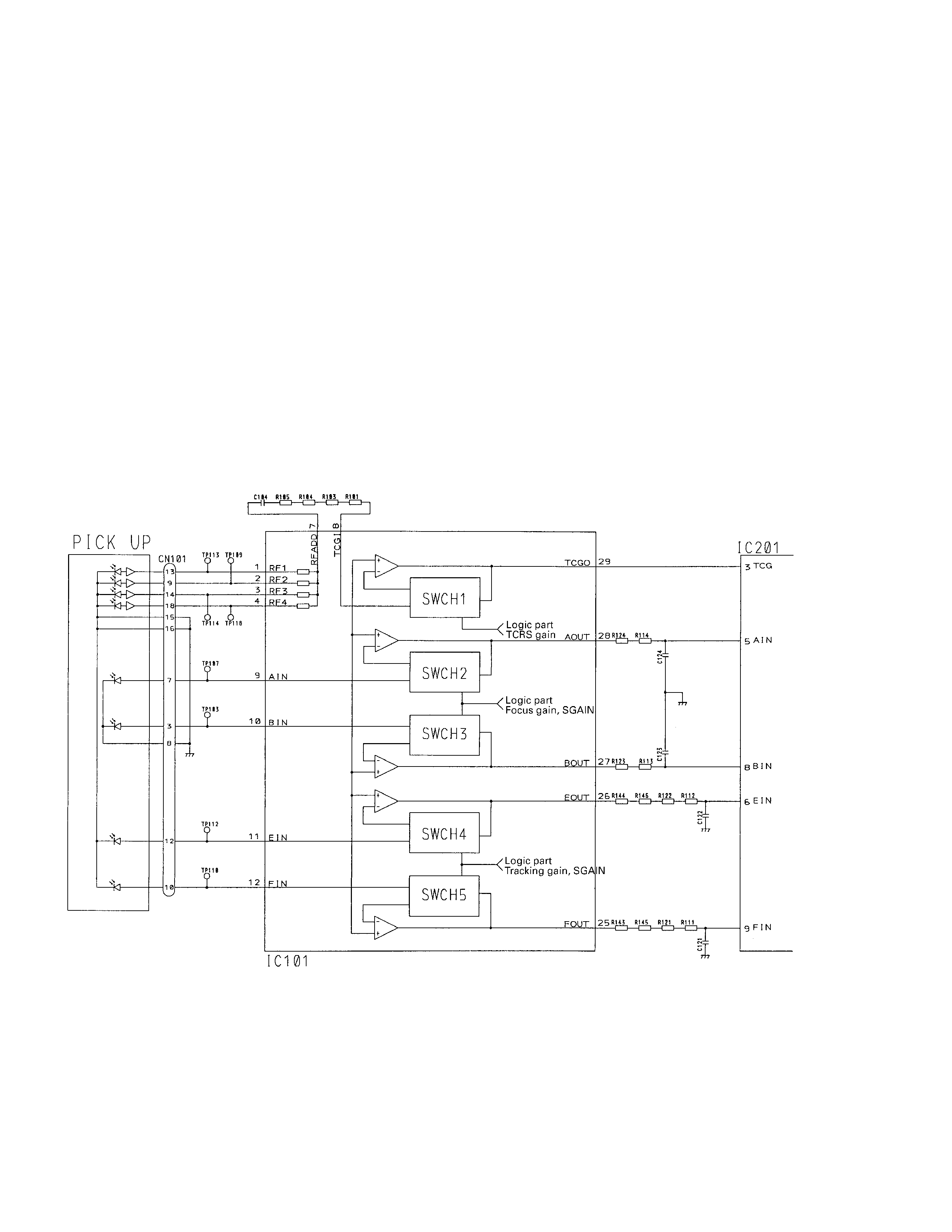
Figure 3 shows the block diagram of this part. The block
generates the ADIP signal which exists only on a
Recordable DISC of a MD.
Signals input to RF1 and RF2 (1,2 pin) are transmitted
through the AGC part and the filter part to be output to
22KO (32 pin). The 22KO is designed to be maintained
at almost same level (approx. 1.2 Vpp) with the AGC
circuit. However, fluctuation of about +0.5V may be
observed due to core components, responsibility of
tracking servo, etc. The signal is then converted to 1
and 0 signal with the comparator C1, input to the signal
processing part (IC201:11 pin), and used for address
control when playing disc for recording and spindle
control.
*Will not be used when Premaster Disc is played.
C1
Fig.3

4
CX-893
Track cross part, signal amplifying part for servo
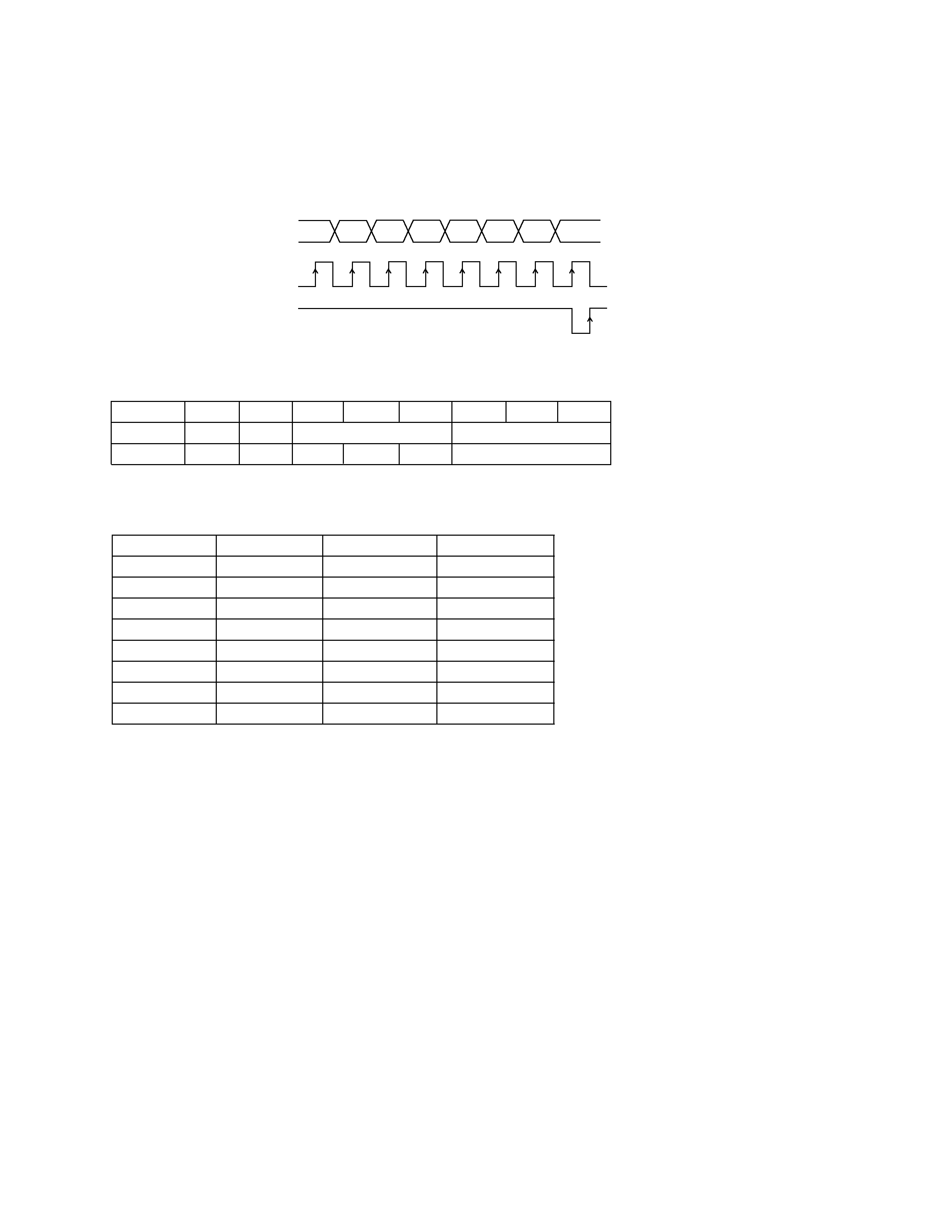
Figure 4 shows the block diagram of these parts.
The signal input to RF1-4 (1-4 pin) is resistive divided
and amplified to be output to TCGO (29 pin). TCGO is
input to the signal processing part (IC201:7 pin) and
TCRS signal is generated and will be used when the
system skips tracks to play.
Outputs from the focus servo based photo diode are
input to AIN (9 pin) and BIN (10 pin) and are output to
AOUT (28 pin) and BOUT (27 pin), respectively, after
being amplified.
Outputs from focus servo based photo diode are input
to EIN (11 pin) and FIN (12 pin) and are output to EOUT
(26 pin) and FOUT (25 pin), respectively, after being
amplified .
These signals are input to the signal processing part
(IC201: 5,6,7,8,9 pin) and used at each servo.
Amplifying ratios of each signal are controlled by the
microprocessor and adjusted so that they reach
optimized values when mechanical modules are
shipped. Those optimized values are stored in IC402.
Therefore, when you replace IC or PU switch, etc., you
should have the IC402 memorize new optimized values
by turning EEPROM (IC402) to write mode (See the
relevant sections for details.) and running test modes
AUTO1 and AUTO2 with a Recordable DISC (MMD-211
or MMD-212).
Fig.4

5
CX-893
Logic part
Serial commands of the microprocessor determines the
setting of this IC.
Timing chart
DATA (23pin)
CLOCK (22pin)
LATCH (21pin)
MSB
7SB
6SB
5SB
4SB
3SB
2SB
1SB
Structure of serial data
MSB
7SB
6SB
5SB
4SB
3SB
2SB
1SB
Pattern A
H
L
Focus gain
Tracking gain
Pattern B
L
H
STBY
DISC
SGAIN Track loss gain
Gain setting (+12dB when SGAIN=H at normal operation)
Setting value
Focus gain
Tracking gain
Track loss gain
000
40
40
18
001
34
34
12
010
28
28
6
011
22
22
0
100
16
16
6
101
10
10
12
110
4
4
18
111
4
4
18
STBY: Switches to stand-by mode
H: Normal L: Stand-by
DISC: Switches to disc mode
H: PIT (Premaster Disc)
L: GRV (Recordable Disc)
SGAIN: Switch of amplifier gain for servo
H: +12dB
L: Normal
