-
This Service Manual outlines operations of the CD mechanism module used in the models listed
blow.
-
For repair, use this Service Manual and the Service Manual of the model used in the system.
Model
Service manual
CD mechanism module
CD mechanism unit
DEX-P1R/UC
DEH-P946/ES
CRT2206
CXK5101
CXB1699
DEX-P1/ES
DEH-P945R/EW
CRT2207
CXK5101
CXB1699
DEX-P99R/EW
CX-680
ORDER NO.
CRT2216
Service
Manual
CD MECHANISM MODULE
CONTENTS
1. CIRCUIT DESCRIPTIONS ........................................... 2
2. MECHANISM DESCRIPTIONS ................................. 15
3. DISASSEMBLY .......................................................... 17
PIONEER ELECTRONIC CORPORATION
4-1, Meguro 1-Chome, Meguro-ku, Tokyo 153-8654, Japan
PIONEER ELECTRONICS SERVICE INC.
P.O.Box 1760, Long Beach, CA 90801-1760 U.S.A.
PIONEER ELECTRONIC [EUROPE] N.V.
Haven 1087 Keetberglaan 1, 9120 Melsele, Belgium
PIONEER ELECTRONICS ASIACENTRE PTE.LTD. 501 Orchard Road, #10-00, Lane Wheelock Place, Singapore 238880
C
PIONEER ELECTRONIC CORPORATION 1998
K-FES. MAY. 1998 Printed in Japan

CX-680
2
1. CIRCUIT DESCRIPTIONS
1.1 Preamplifier (UPC2572GS: IC101)
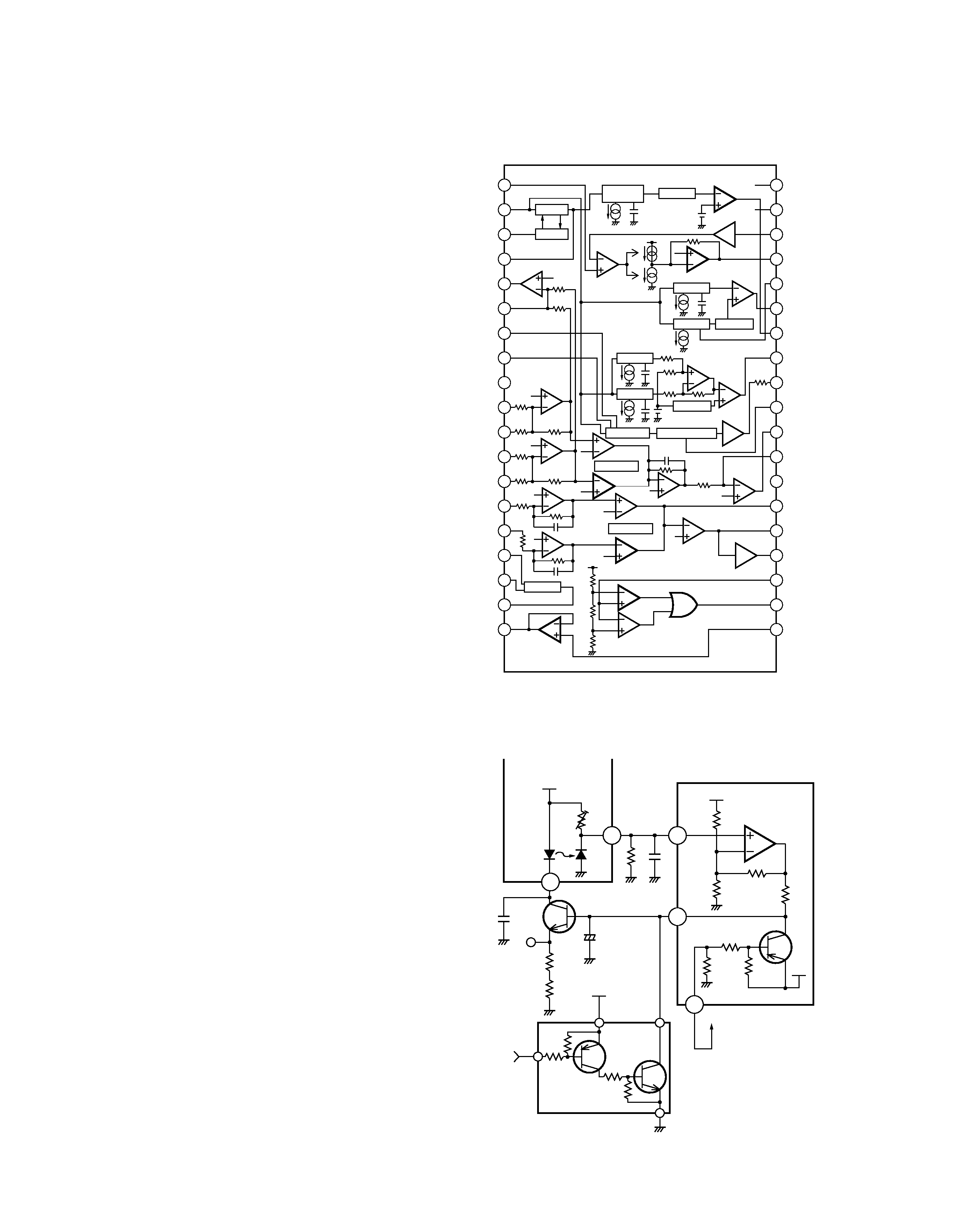
Fig. 1 Block Diagram of UPC2572GS
Fig. 2 APC Circuit
The preamplifier processes pickup output signals to
generate signals to be sent to the servo, demodula-
tor, and controller. The preamplifier with built-in
photodetector converts signals from the pickup into
intermediate voltage in the pickup. Then, addition is
made in the RF amplifier (IC101) to obtain RF, FE, TE,
and TE zero cross signals. The system consists of the
UPC2572GS and other components explained below.
The system uses a single power source (+5 V). There-
fore, the reference voltage of IC101 and the reference
voltage of the power unit and servo circuit are REFO
(+2.5 V). REFO is obtained from REFOUT of servo LSI
(IC201: UPD63702GF) via a buffer, and is output from
Pin 19 of IC101. This REFO is used as reference for all
measurements.
Note: Do NOT short-circuit REFO and GND during
measurement.
1
2
3
4
5
6
7
8
9
10
11
12
13
14
15
16
17
18
19
38
37
36
35
34
33
32
31
30
29
28
27
26
25
24
23
22
21
20
X12
RF
envelope
AGC
Detection
X3
Phase detection
3T detection
Bottom
DC shift
Peak
Control
DC shift
Bottom
Peak
120k
DEFECT circuit
FE BAL
FE
BAL
Vcc
Mirror circuit
FE BAL
APC
X2
Vcc
FE-BAL
TE-BAL
ASY
EFM-OUT
C.DEF
DEFECT
RFOK
MIRR
3T-OUT
C.FE
FE-OUT
FE-
GND
TE-
TE-OUT1
TE-OUT2
DET-IN
DET-OUT
VREF-IN
VREF-OUT
LDON
LD
PD
E
F
D
B
C
A
Vcc
C2.3T
C1.3T
RF-
RF-OUT
RF-IN
C AGC
AGC-OUT
EFM-IN
HPF
TE
BAL
EFM comparator
Control
1) Automatic Power Control (APC) circuit
Laser diode has negative temperature characteristics
with great optical output when the diode is driven
with constant current. Therefore, current must be
controlled by a monitor diode to ensure constant out-
put. Thus functions the APC circuit. LD current can be
obtained by measuring the voltage between LD1 and
GND. The current value is approximately 35 mA.
Vcc (5V)
Vr
LD
MD
UPC2572GS
16
PD
17
LD
15
Q101
2SD1664
C124
0.1
µF
C101
(100
µF/6.3V)
R101
10
LD1
R102
12
5V
CONT
Q102 UMD2N
18
5V
5V
1k
150k
16k
R112
2.2k
C104
0.33
µF
5
1k
2.5V
Pickup unit

CX-680
3
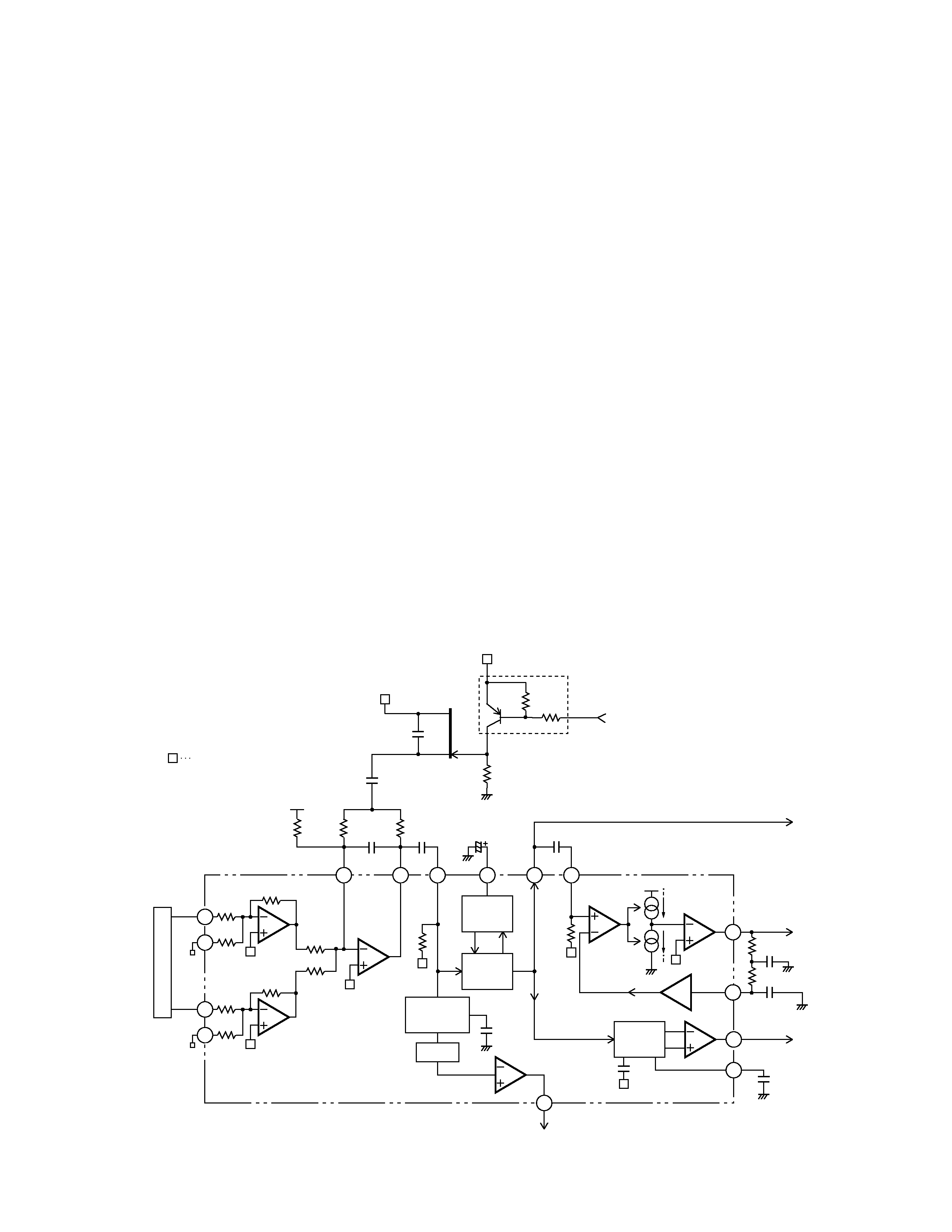
2) RF amplifier and RF AGC amplifier
Photodetector outputs (A+C and B+D) are added, am-
plified and equalized in IC101, and output to the RFI
terminal as RF signal. (Eye pattern can be checked at
this terminal.)
Low-frequency components of voltage RFI is:
RFI = (A + B + C + D) x 3.22
where R111 is offset resistor to keep RFI signal within
the output range of the preamplifier. RFI signal is
goes under AC coupling, and is input to Pin 4 (RFIN
terminal).
IC101 contains an RF AGC circuit. RFO output from
Pin 2 is maintained to a constant level (1.2
±0.2 Vp-p).
The RFO signal is used in the EFM, DFCT, and MIRR
circuits.
3) EFM circuit
The EFM circuit converts RF signal into digital sig-
nals of "0" and "1." RFO signal after AC coupling is
input to Pin 1, and supplied to the EFM circuit.
Asymmetry caused during manufacturing of discs
cannot be eliminated solely by AC coupling. There-
fore, the system controls the reference voltage ASY
of the EFM comparator by using the fact that proba-
bility to generate "0" and "1" is 50% in EFM signal.
This reference voltage ASY is generated by output
from the EFM comparator through L.P.F. EFM signal
is output from Pin 35. As signal level, amplification is
2.5 Vp-p around REFO.
4) DFCT (defect) circuit
DFCT signal detects mirror defect in discs, and is out-
put from Pin 33. The system outputs "H" when a mir-
ror defect is detected.
If disc is soiled, the system determines it as lack of
mirror. Therefore, the system inputs the DFCT signal
output to the HOLD terminal of servo LSI. Focus and
tracking servo drives change to Hold status only
when DFCT output is in "H" so that performance of
the system upon detection of defect can be im-
proved.
5) RFOK circuit
The RFOK circuit outputs signal to show the timing of
focus closing servo, as well as the status of focus
closing during playback. The signal is output from
Pin 32. The system inputs the RFOK signal output to
the RFOK terminal of servo LSI. The servo LSI issues
Focus Close command. The system outputs signal in
"H" during focus closing and playback.
CN101
12
7
DETECT
13
11
10
10k
20k
9.3k
RFI
+5V
R111
27k
Vcc
×12
ASY
13
20k
(RF AGC)
AGC
RF
ENVELOPE
HPF
VDC
RFOK
20k
33
36
35
34
PEAK
DEFECT
EFM
UPC2572GS
A+C
10k
B+D
9.3k
20k
10k
10k
R105
6.8k
C125 3pF
C105
47pF
C128
33P
R123
10K
Q103
2SK303
Q104
UN2111
R104
8.2k
RFIN
C107
4.7
µF/35V
C122
0.1
µF
C106
RFO
REFO (+2.5V)
DEFECT
BOTTOM
R107 8.2k
R106 18k
C111 3300pF
C110
C112 0.047
µF
6
54
3
21
32
0.1
µF
0.01
µF
1 2
3
SCONT
CWX2165
(CXK5121)
Fig. 3 RF AMP, RF AGC, EFM, DFCT, RFOK Circuit

CX-680
4
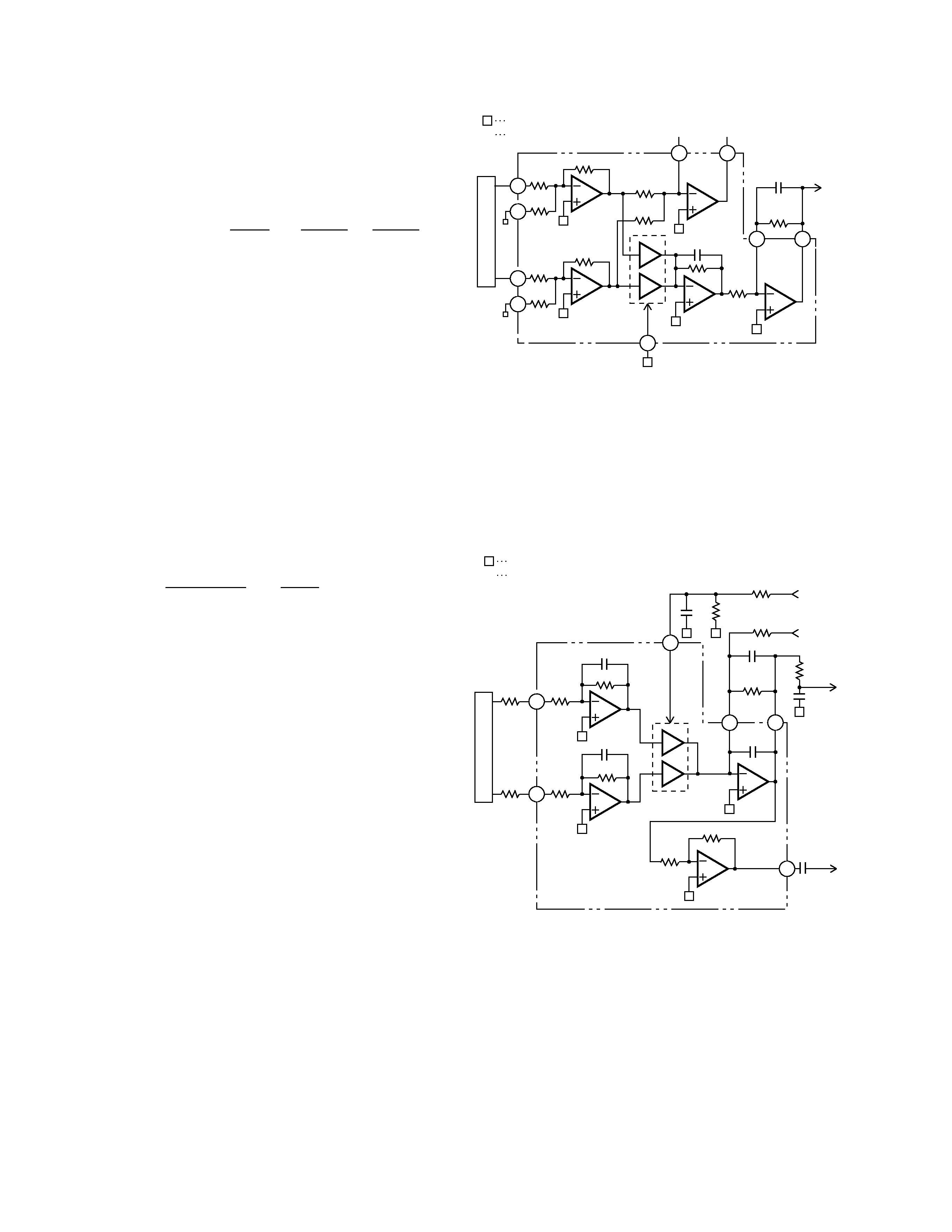
7) Tracking-error amplifier
Outputs E and F from the photodetector are output as
TE signal (E-F) from Pin 24 via the difference amplifi-
er, then via the error amplifier.
Low-frequency components of voltage TEY is:
TE waveforms equivalent to approximately 1.5 Vp-p
are obtained at TE output (Pin 24) by using REFO as
reference. The cut-off frequency of the amplifier of
the last layer is 19.5 kHz.
8) Tracking zero-cross amplifier
Tracking zero-cross signal (TEC signal) is generated
by amplifying TE waveforms (voltage at Pin 24) by a
factor of four. The signal is used for detecting the
zero-cross point of tracking error in the servo LSI
UPD63702GF. The purposes of detecting the zero-
cross point are as follows:
(1) To be used for counting tracks for carriage move
and track jump.
(2) To be used for detecting the direction of lens
movement when tracking is closed. (To be used in
the tracking brake circuit mentioned later.)
The frequency range of TEC signal is from 500 Hz
to 19.5 kHz.
Voltage TEC = TE level x 4
In other words, the TEC signal level is calculated as 6
Vp-p. This level exceeds the D range of the operation
amplifier, resulting in the signal to clip. However,
there shall be no problem, since the servo LSI uses
only zero-cross point.
6) Focus-error amplifier
The system outputs photodetector output (A+C and
B+D) as FE signal (A+C-B-D) from Pin 28 via the dif-
ference amplifier, then via the error amplifier.
Low-frequency components of voltage FEY is:
An S curve equivalent to approximately 1.6 Vp-p is
obtained at FE output (Pin 28) by using REFO as refer-
ence. The cut-off frequency of the amplifier of the
last layer is 12.4 kHz.
Fig. 4 Focus-error amplifier
Fig. 5 Tracking-error amplifier,
Tracking zero-cross amplifier
CN101
R117
16k
R116
16k
14
15
9
11
31k
31k
50pF
63k
C123
4.7nF
R114
10k
R113
10k
TBAL
C115
120pF
R109
68k
R115
1k
C126
15nF
TEY
4R
R
F
E
23
TEC
C116
6.8nF
TE VCA
gm=1/17k
63k
37
24
5pF
TOFST
R110
130k
50pF
25
REFO (+2.5V)
gm
CONDUCTANCE
UPC2572GS
65
RFO
9.3k
9.3k
20k
10k
10k
7
13
12
13
10k
10k
20k
FE VCA
38
REFO
C114
390pF
FE
R108
33k
28
FE
27
R
17.2k
50pF
gm=1/68.8k
90k
10
11
CN101
A+C
B+D
F.BAL
REFO (+2.5V)
gm
CONDUCTANCE
UPC2572GS
20k
90k
R108
FEY=(A+CBD)X
X
X
10k
68.8k
17.2k
: (FE level of pickup unit x 5.02)
63k
R109
TEY=(EF) X
X
31k
+16k
17k
: (TE level of pickup unit x 5.36)

CX-680
5
RFO
PEAK HOLD
BOTTOM HOLD
MIRROR
1
A
0
False MIRR caused by dirt
True MIRR
OFF TRACK
Dirt, etc.
B
C
Z
Ø
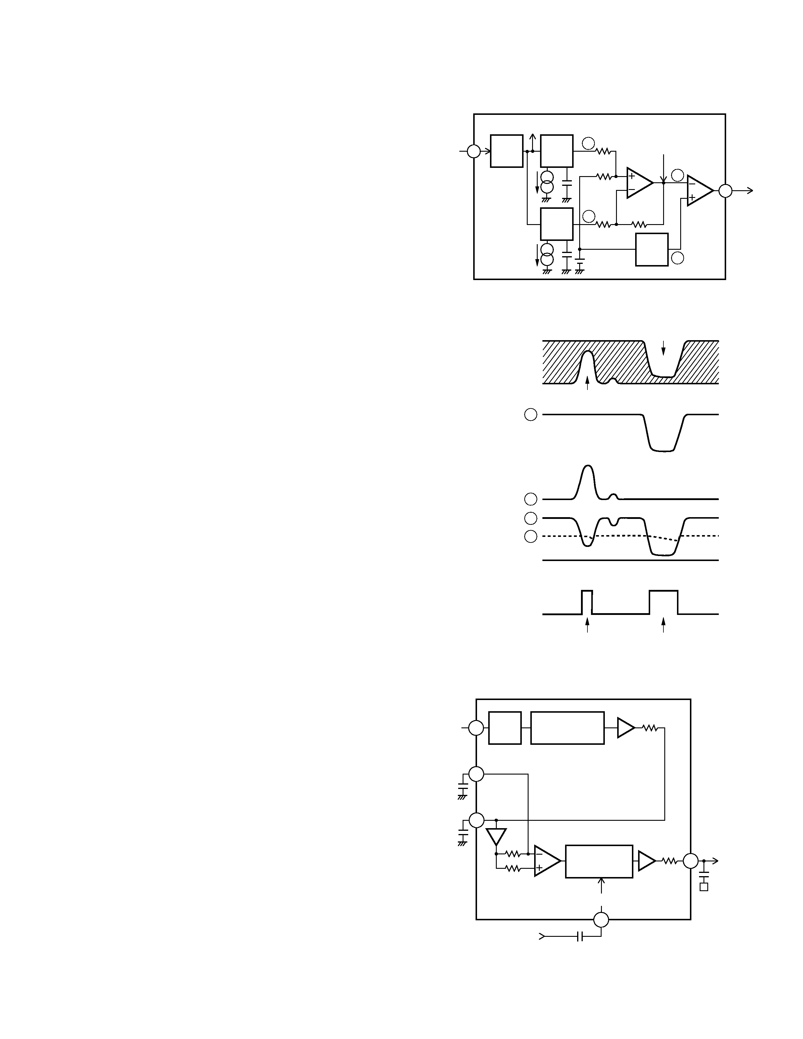
Fig. 8 3T OUT Circuit
Fig.6 MIRR Circuit
Fig. 7 MIRR Circuit
9) MIRR (mirror) circuit
MIRR signal shows ON and OFF track information.
The signal is output from Pin 31.
The status of MIRR signal is as follows:
Laser beam ON track: MIRR = "L"
Laser beam OFF track: MIRR = "H"
The signal is used in the brake circuit mentioned lat-
er.
3T-OUT
FE signal
RFIN
UPC2572GS
C113
10nF
FEY
3T detection
C117
0.033
µF
120k
L.P.F
Phase detection
8
+
H.P.F
10k
10k
1k
C2.3T
C109
100pF
C1.3T
C108
0.027
µF
8
7
30
29
4
AGC
Differential
rectification
3T LEVEL ENVELOPE
DETECTOR
Phase
comparison
10) 3T OUT circuit
The system detects flickering of RF signal when dis-
turbance is input to the focus servo loop, and outputs
the difference of phase between FE signal and RF-
level fluctuation signal from Pin 30. The resulting sig-
nal is obtained through L.P.F. with a fc of 40 Hz. This
signal is used for automatic adjustment of FE bias.
MIRR
COMP
DC
shift
Peak
AGC
Bottom
RFO Detection
A
1.5V
UPC2572GS
(Peak) (Bottom)
4
31
RFIN
B
Z
C
