© 2000-12 PRINTED IN JAPAN
B51-8558-00 (N) 889
ALL MODE MULTI-BAND TRANSCEIVER
TS-2000/X
SERVICE MANUAL
CIRCUIT DESCRIPTION ............................. 2
DESCRIPTION OF COMPONENTS ......... 24
SEMICONDUCTOR DATA ....................... 34
PARTS LIST .............................................. 51
EXPLODED VIEW ..................................... 93
PACKING .................................................. 97
ADJUSTMENT ......................................... 98
TERMINAL FUNCTION .......................... 124
WIRING .................................................. 133
PC BOARD VIEWS / CIRCUIT DIAGRAMS
FILTER UNIT (X51-315X-XX) ............. 135
FINAL UNIT (X45-360X-XX) .............. 137
DISPLAY UNIT (X54-3320-00) ........... 151
CONTROL UNIT (X53-391X-XX) ....... 155
TX-RX 1 UNIT (X57-605X-XX) ........... 169
TX-RX 2 UNIT (X57-606X-XX) ........... 186
TX-RX 3 UNIT (X57-6070-00) ............ 209
BLOCK DIAGRAM .................................. 223
LEVEL DIAGRAM ................................... 229
MC-52DM ............................................... 233
UT-20 ..................................................... 235
RC-2000 ................................................. 235
ARCP-2000 ............................................ 235
SPECIFICATIONS ................................... 236
Knob
(K21-1104-03)
Knob ring
(K29-5395-04)
Knob
(K29-5397-13) x 2
Knob
(K29-5398-03) x 3
Knob
(K29-5399-03) x 3
Knob
(K29-5396-03) x 2
Key top
(K29-5391-02)
Key top
(K29-5393-12)
Key top
(K29-5394-12)
Key top
(K29-5392-12)
Front glass
(B10-2608-02)
Cabinet (Upper)
(A01-2176-01)
Foot
(J02-0442-04) x 2
Foot
(J02-0440-04)
RF coaxial receptacle (Round)
(E06-0858-15)
Phone jack (9P)
(E11-0438-05)
CONTENTS

2
TS-2000/X
Overview of the Operation
The TS-2000/X basically consists of an all-mode-receiver
incorporating an IF/AF DSP for satellite communication with
an independent FM/AM sub-receiver for the VHF and UHF
bands.
s Overview of the operation of the all-mode trans-
ceiver unit (main band side) with an IF/AF DSP
for satellite communication
The receiver unit has an independent front end for each
of the HF, 50MHz, 144MHz, 430MHz and 1.2GHz bands
(some products do not support the 1.2GHz band). The cir-
cuits following the 10.695MHz IF stage are common to all
the bands. (Thus, it cannot receive two SSB signals at the
same time.)
The IF frequency of the transmitter unit is shifted from
the IF frequency of the receiver unit by 100kHz to enable
satellite operation (full duplex operation). The final section is
independent of the HF, 50MHz, 144MHz, 430MHz and
1.2GHz bands. Consequently, you can select a combination
of bands permitting satellite communication from the HF,
50MHz, 144MHz, 430MHz and 1.2GHz bands.
The transmitter unit and receiver unit on the main band
side operate simultaneously during satellite transmission.
The receiver unit on the sub-band side does not work. (The
sub-band receiver is not used during satellite operation.)
Two 16-bit DSP ICs are used; one performs IF processing
(main band side) and the other carries out AF processing
(main and sub bands). Although the DSP IC is a 16-bit unit, it
carries out "double-precision operations" for critical parts of
IF processing to perform 32-bit equivalent processing. In
addition, the DSP IC uses a 100-MHz high-speed internal
clock. The conversion from an analog signal to a digital sig-
nal (A/D conversion) is performed with 24 bits at high preci-
sion.
The DSP circuit for IF operates in any mode other than
FM mode for both transmission and reception. FM modula-
tion, detection and squelch processing are conventional ana-
log processes. (The processing prior to modulation and af-
ter demodulation in FM is performed by the DSP.)
In the mode in which the IF DSP circuit operates, it car-
ries out modulation and demodulation, digital IF filtering,
digital AGC, and CW waveform processing during transmis-
sion, as in the TS-870. All these functions are operated in all
the bands on the main band side, including satellite opera-
tion.
The AF unit is processed by the DSP in all modes. The
operating range of the DSP circuit depends on the mode,
but it performs beat cancellation, noise reduction, AF DSP
filtering, etc.
s Overview of the operation of the independent
FM/AM sub-receiver unit (sub-band side) for the
VHF and UHF bands
The local oscillator system and IF/AF signal system of the
sub-receiver unit are independent of the main band side.
Therefore, the sub-band receiver can receive signals while
the main band receiver is sending a signal. (Except when
reception is impossible due to harmonics of the transmit fre-
quency and when the main band and sub-band are on the
same frequency band.)
The sub-band receive signal is branched from the RF unit
on the main band side. It is, therefore, not necessary to
install a dedicated antenna for sub-band reception.
Transmission can be performed with the sub receive fre-
quency by shifting the "PTT band" to the sub-band side. It
is made possible by internally using the transmission func-
tion on the main band side.
AF processing is also carried out by the DSP on the sub-
band side and the noise reduction function works.
The sub-band reception function, including display, can
be turned off.
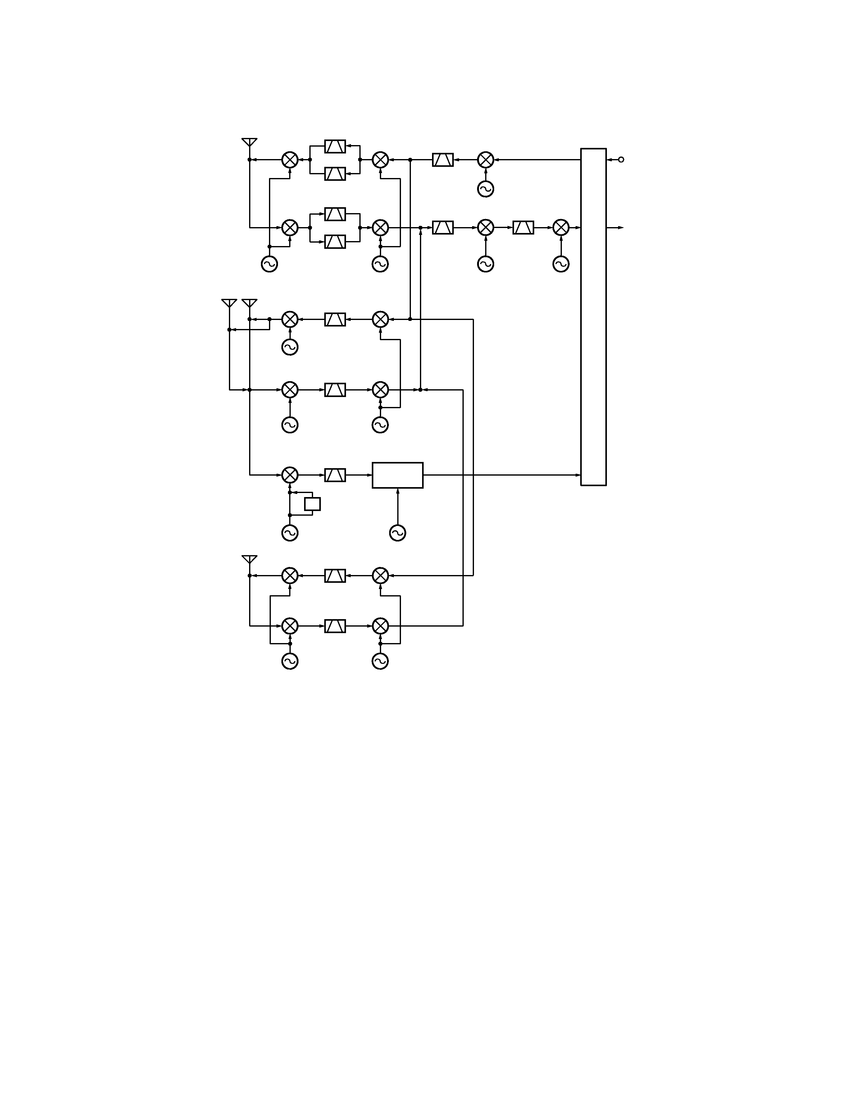
Frequency Configuration (Fig. 1)
This transceiver utilizes double conversion in FM mode
and triple conversion in non-FM modes during transmission.
It utilizes triple conversion in FM mode and quadruple
conversion in non-FM modes during reception. The fourth
12kHz IF signal is converted from analog to digital and con-
nected to the DSP.
When the carrier point frequency of the signal input from
the antenna is fIN, the relationship between these signals
when demodulating this signal is expressed by the following
equations:
HF MAIN
fIN = fLO1 fLO2 fLO3 + fLO4 12kHz
VHF MAIN
fIN = fLO1 fLO2 fLO3 + fLO4 12kHz
UHF MAIN
fIN = fLO1 + fLO2 + fLO3 fLO4 + 12kHz
1.2G MAIN fIN = fLO1 x 2 + fLO2 + fLO3 fLO4 + 12kHz
Reference Signal Generation Circuit
The 15.6MHz reference frequency fstd for PLL frequency
control is generated by the TCXO (X400). The signal passes
through a buffer amplifier (Q420) and is used as the refer-
ence signal for the second local oscillator (HFLO2) for HF
band reception and the first local oscillator (SLO1) subband
reception.
The reference signal is doubled by Q412, and the result-
ing 31.2MHz signal is used as the reference signal for DDSs
(IC406, IC407, IC408, IC601, IC602, IC603).
The 31.2MHz signal is supplied to the TX-RX2 unit (X57-
606 A/11) as LO2 for VHF and UHF bands.
CIRCUIT DESCRIPTION

3
TS-2000/X
68.985MHz
75.825MHz
TX MIX
TX MIX
TX MIX
TX MIX
TX MIX
69.085MHz
10.695MHz
10.595MHz
75.925MHz
RX MIX
RX MIX
RX MIX
DET
TCAR
10.583MHz
455kHz
LO3
11.150MHz
LO1HF
75.955~
129.085MHz
LO2
58.390~
65.230MHz
RCAR
467kHz
41.795MHz
LO1TX
183.795~418.205MHz (K)
185.795~398.205MHz (E)
RX MIX
RX MIX
41.895MHz
SUB
RX MIX 58.525MHz
LO1RX
183.895~
418.105MHz (K)
185.895~398.105MHz (E)
SLO2
58.070MHz
TX MIX
TX MIX
135.395MHz
RX MIX
RX MIX
135.495MHz
1.2GLO1
1104~
1165MHz
LO31
31.2MHz
Mixer
IF detector
÷2
SLO1
322.95~
465.04MHz (K)
371.475~409.050MHz (E)
HF/
50MHz
UHF
VHF
1.2G
1.2GLO2
124.8MHz
DSP
MIC
input
AF
output
HF/50MHz LO1
When the HF and or 50MHz band is operating in the main
band, the HF REF VCO (Q427) generates 31.17 to 32.834
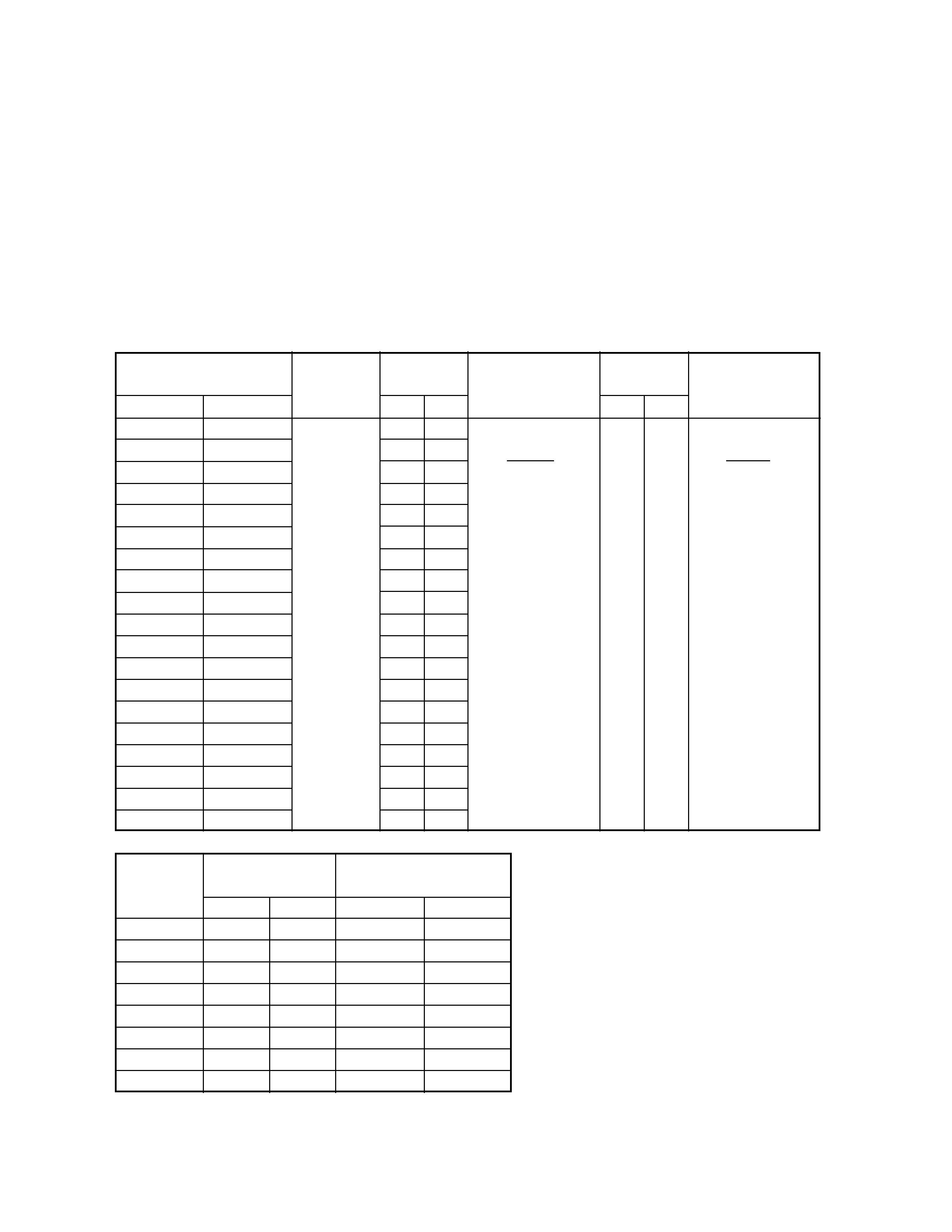
MHz. (See Table 1, frequency configuration.)
The output signal from the DDS (IC408) is input to pin 8
of the PLL IC (IC409) for HF REF, divided into 1/16 in IC409
to produce comparison frequency fø 2 of 487 to 513kHz.
The output signal from the VCO (Q427) goes to pin 6 of
PLL IC (IC409), is divided into 1/64 in IC409, and compared
with the signal with comparison frequency fø 2 by a phase
comparator. The frequency is locked and the HF REF signal
is output.
The output signal from the PLL IC (IC409) for HF REF is
fed to pin 8 of the PLL IC (IC414) for HF LO1 as a reference
frequency, and divided to produce comparison frequency
fø 1 of 975 to 1358kHz.
The HF LO1 VCO (Q459, Q460, Q464) generates 75.955
to 129.185MHz. The output from this VCO goes to pin 6 of
IC414, is divided into 1/N 1 in IC414, compared with the sig-
nal with comparison frequency fø 1 by a phase comparator.
The frequency is locked and the HF LO1 output frequency is
generated.
The DDS (IC408) sweeps output frequency (7.792 to
8.209MHz) in 10Hz steps by equation fDDS STEP (Hz) =
(10*R 1)/(N 1*4) and in 1Hz steps by equation fDDS STEP
(Hz) = (1*R 1)/(N 1*4), the HF LO1 covers the frequencies
of 75.955 to 129.085MHz in 10Hz or 1Hz steps.
One of three VCOs (Q459, Q460, Q464) is selected by
the signal (HF VCO1,HF VCO2,HF VCO3) from the serial-par-
allel IC (IC404).
The output from the VCOs (Q459, Q460, Q464) passes
through a buffer amplifier (Q462), is amplified by Q476, and
passes through a low-pass filter. The impedance is con-
verted by an attenuator and the signal is output as HFLO1.
The cut-off frequency of the low-pass filter in the output
section is changed by turning Q474 ON/OFF with a VCO se-
lect signal (HF VCO1).
Fig. 1
Frequency configuration
CIRCUIT DESCRIPTION

4
TS-2000/X
HF LO2
When the HF and or 50MHz band is operating, the
HF LO2 VCO (Q409) generates 65.230 to 58.390MHz. (See
Table 1, frequency configuration.)
The 15.6MHz reference signal fstd is input to pin 8 of the
PLL IC (IC401) for HF LO2, divided into 1/226 and 1/319 in
IC401 to produce comparison frequency fø of 69.027 to
48.903kHz.
The output signal from the VCO (Q409) goes to pin 6 of
IC401, its frequency is divided into 1/945 and 1/1194 in
IC401, compared with comparison frequency fø by a phase
Display frequency
LO1 OUT
IC414 :
HF REF
IC409 :
DDS output (MHz)
fRX (MHz)
(MHz)
LMX2306TMX
(MHz)
LMX2306TMX
IC408 : AD9835BRU
Start
Stop
R1
N1
N2
R2
0.030000
1.999999
LO1
32
76
HF REF
64
16
fDDS
2.000000
5.999999
= fRX + IF
30
75
=
(fRX + IF)
*R1
=
HF REF
*R2
6.000000
8.999999
32
84
N1
N2
9.000000
12.999999
30
75
13.000000
16.999999
32
84
17.000000
17.999999
32
92
18.000000
21.999999
30
90
22.000000
23.999999
32
100
24.000000
24.999999
32
92
25.000000
25.999999
30
90
26.000000
29.999999
24
78
30.000000
32.999999
32
100
33.000000
36.999999
30
97
37.000000
40.999999
32
115
41.000000
44.999999
32
119
45.000000
48.999999
30
115
49.000000
51.999999
30
113
52.000000
55.999999
30
115
56.000000
60.000000
32
127
LO2 OUT
IC401 :
IF
(MHz)
LMX2306TMX
N3
R3
RX
TX
65.230088
945
226
75.925088
75.825088
58.389969
1194
319
69.084968
68.984968
65.230088
945
226
75.925088
75.825088
58.389969
1194
319
69.084968
68.984968
65.230088
945
226
75.925088
75.825088
58.389969
1194
319
69.084968
68.984968
65.230088
945
226
75.925088
75.825088
58.389969
1194
319
69.084968
68.984968
comparator, and locked. The division ratio data comes from
the control unit.
The output signal from the VCO (Q409) passes through a
buffer amplifier (Q415), is amplified by Q421, and passes
through a low-pass filter. The impedance is converted by an
attenuator and the signal is output as HF LO2.
When the HF and or 50MHz band is not operating, Q403
is turned OFF with the LO2SEL signal and HF LO2 VCO
(Q409) stops operation.
Table 1
Main HF and 50MHz band frequency configuration
CIRCUIT DESCRIPTION

5
TS-2000/X
144MHz LO1
When the VHF band is operating in the main band, the
VHF REF VCO (Q441) generates 36.057 to 37.288MHz (K),
36.450 to 36.842MHz (E). (See Table 2, Frequency Configu-
ration.)
The output signal from the DDS (IC406) is input to pin 8
of the PLL IC (IC411) for VHF REF and divided into 1/16 in
IC411 to produce comparison frequency fø 2 of 563 to
583kHz (K), 569 to 576kHz (E).
The output signal from the VCO (Q441) goes to pin 6 of
IC411 and its frequency is divided into 1/64 in IC411, com-
pared with the signal with comparison frequency fø 2 by a
phase comparator, and is locked.
The VHF REF PLL output signal is fed to pin 8 of IC410 as
a reference frequency, and divided into 1/30 in IC410 to pro-
duce comparison frequency fø 1 of 1202 to 1243kHz (K),
1215 to 1228kHz (E).
The VHF LO1 VCO (Q433) generates 183.895 to 193.895
MHz (K), 185.795 to 187.895MHz (E) in receive mode and
183.795 to 193.795MHz (K), 185.795 to 187.795MHz (E).
The VCO (Q433) output signal goes to pin 6 of IC410, and
its frequency is divided into 1/N1 in IC410 and compared
with comparison frequency fø 1 by a phase comparator. The
frequency is locked and LO1 is generated.
The DDS (IC406) sweeps output frequency (9.014 to
Display frequency
LO1 OUT
IC410 :
VHF REF
IC411 :
DDS output (MHz)
fRX (MHz)
(MHz)
LMX2306TMX
(MHz)
LMX2306TMX
IC406 : AD9835BRU
Start
Stop
R1
N1
N2
R2
142.000000 (K) 146.999999 (K)
LO1
30
153
VHF REF
64
16
fDDS
144.000000 (E) 146.000000 (E)
= fRX + IF
=
(fRX + IF)
*R1
=
VHF REF
*R2
147.000000 (K) 151.999999 (K)
156
N1
N2
IF = RX : 41.895
TX : 41.795
9.321MHz (K), 9.112 to 9.210MHz (E)) in 10Hz steps by
equation fDDS STEP (Hz) = (10*R1)/(N1*4) and in 1Hz steps
by equation fDDS STEP (Hz) =(1*R1)/(N1*4), the LO1 covers
the frequencies of 183.895 to 193.895 MHz (K), 185.895 to
187.895MHz (E) in receive mode and 183.795 to
193.795MHz (K), 185.795 to 187.795MHz (E) in transmit
mode in 10Hz or 1Hz steps.
The PLL output signal is changed by the switching circuit
of Q469 (receive) and Q470 (transmit) so that the output
amplifier and low-pass filter correspond to VHF band trans-
mission and reception.
In receive mode, the signal is amplified by the broad-
band amplifier (IC415), and passes through a low-pass filter.
The impedance is converted by an attenuator and the signal
is output to the RF unit (X57-606) as the first local oscillator
RXLO1.
In transmit mode, the signal is amplified by the broad-
band amplifier (IC416), and passes through a low-pass filter.
The impedance is converted by an attenuator and the signal
is output to the RF unit (X57-606) as the first local oscillator
TXLO1.
When the VHF is not operating, Q436 is turned OFF with
a signal from the serial-parallel IC (IC404) and VHF LO1 VCO
(Q433) stops operation.
430MHz LO1
When the UHF band is operating in the main band, the
UHF REF VCO (Q431) generates 378.105 to 418.105MHz
(K), 388.105 to 398.105MHz (E) in receive mode and
378.205 and 418.205MHz (K), 388.205 to 398.205MHz (E).
(See Table 3, Frequency Configuration.)
The output signal (8.328 to 8.475MHz (K), 8.344 to
8.469MHz (E)) from the DDS (IC407) passes through a ce-
ramic filter (CF400), is input to pin 8 of the PLL IC (IC412) for
UHF and divided into 1/16 in IC412 to produce comparison
frequency fø of 520 to 530 kHz.
The output signal from the VCO (Q431) goes to pin 6 of
IC412 and its frequency is divided into 1/N in IC412, com-
pared with comparison frequency fø by a phase comparator,
and is locked.
The DDS (IC407) sweeps output frequency (8.328 to
8.475MHz (K), 8.344 to 8.469MHz (E)) in 10Hz steps by
equation fDDS STEP (Hz) = 10*R/N and in 1Hz steps by equa-
tion fDDS STEP (Hz) = 1*R/N, the LO1 covers the frequencies
of 378.105 to 418.105MHz (K), 388.105 to 398.105MHz (E)
in receive mode and 378.205 to 418.205MHz (K), 388.205 to
398.205MHz (E) in transmit mode in 10Hz or 1Hz steps.
The PLL output signal is changed by the switching circuit
of Q471 (receive) and Q472 (transmit) so that the output
amplifier and low-pass filter correspond to UHF band trans-
mission and reception.
In receive mode, the signal is amplified by the broad-
band amplifier (IC415), and passes through a low-pass filter.
The impedance is converted by an attenuator and the signal
is output to the RF unit (X57-606) as the local oscillator sig-
nal RXLO1.
In transmit mode, the signal is amplified by the broad-
band amplifier (IC416), and passes through a low-pass filter.
The impedance is converted by an attenuator and the signal
is output to the RF unit (X57-606) as the local oscillator sig-
nal TXLO1.
When the UHF is not operating, Q434 is turned OFF with
a signal from the serial-parallel IC (IC404) and UHF VCO
(Q431) stops operation.
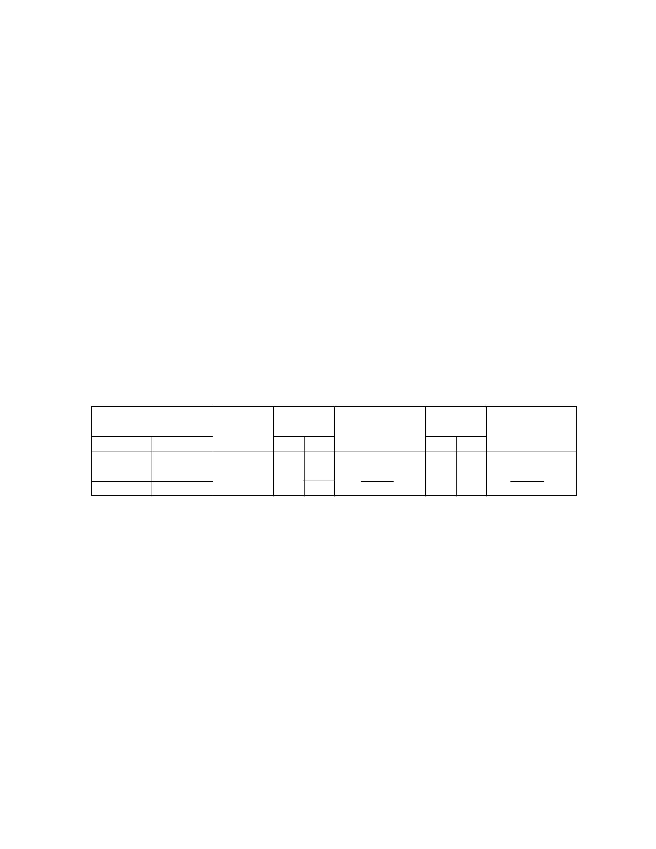
Table 2
Main VHF band frequency configuration
CIRCUIT DESCRIPTION
