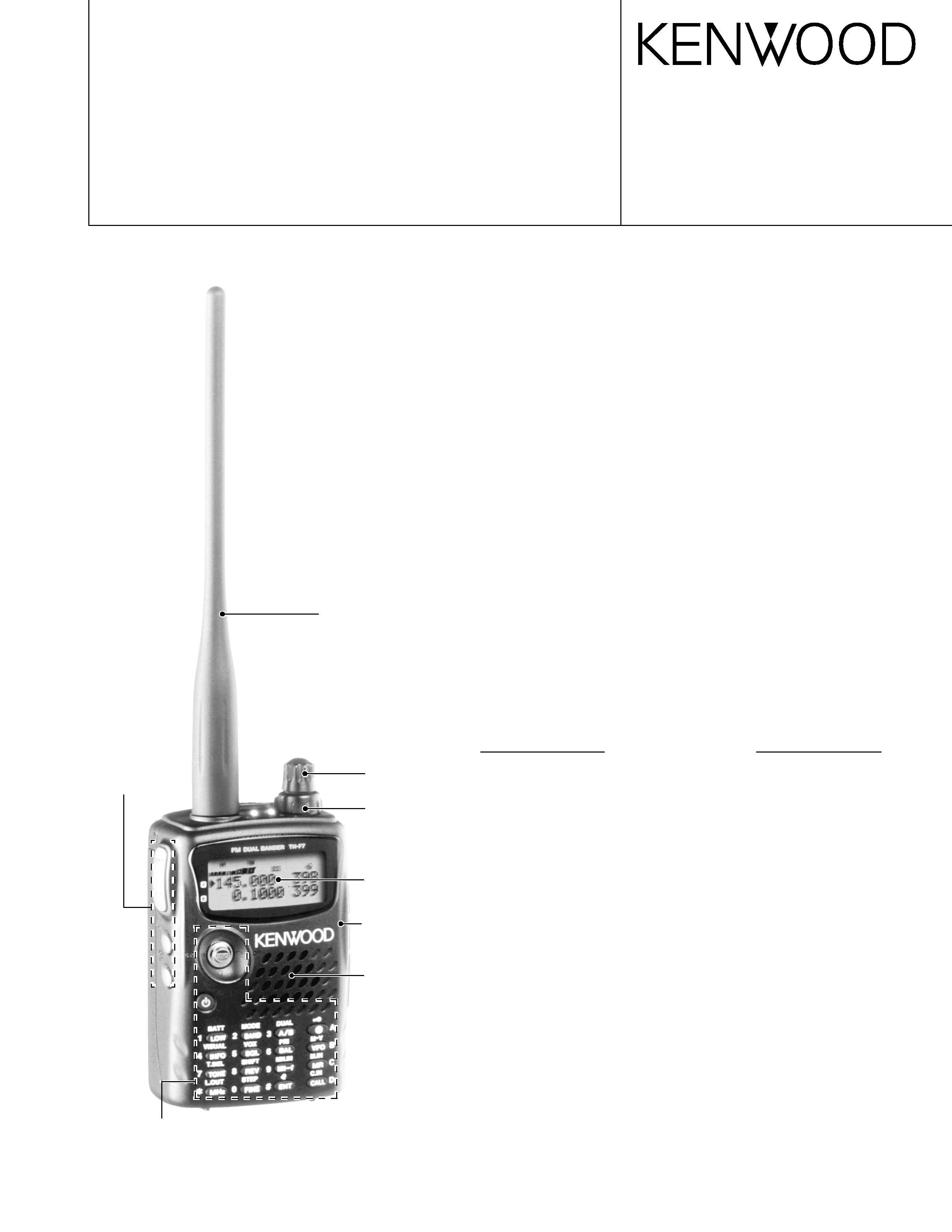
144/220/440MHz FM TRIBANDER / 144/430MHz FM DUAL BANDER
TH-F6A/F7E
© 2001-8 PRINTED IN JAPAN
B51-8580-00 (S) 798
SERVICE MANUAL
DISASSEMBLY FOR REPAIR .................................................. 2
CIRCUIT DESCRIPTION .......................................................... 4
DESCRIPTION OF COMPONENTS ....................................... 14
PARTS LIST ............................................................................ 19
EXPLODED VIEW .................................................................. 32
PACKING ................................................................................ 33
ADJUSTMENT ........................................................................ 34
PC BOARD VIEWS
TX-RX UNIT (CONTROL SECTION) ...................................... 59
TX-RX UNIT ............................................................................ 65
TX-RX UNIT (VCO SECTION) ................................................ 71
SCHEMATIC DIAGRAM ......................................................... 73
BLOCK DIAGRAM .................................................................. 81
LEVEL DIAGRAM ................................................................... 83
OPTIONS ................................................................................ 85
SPECIFICATIONS .................................................................. 86
CONTENTS
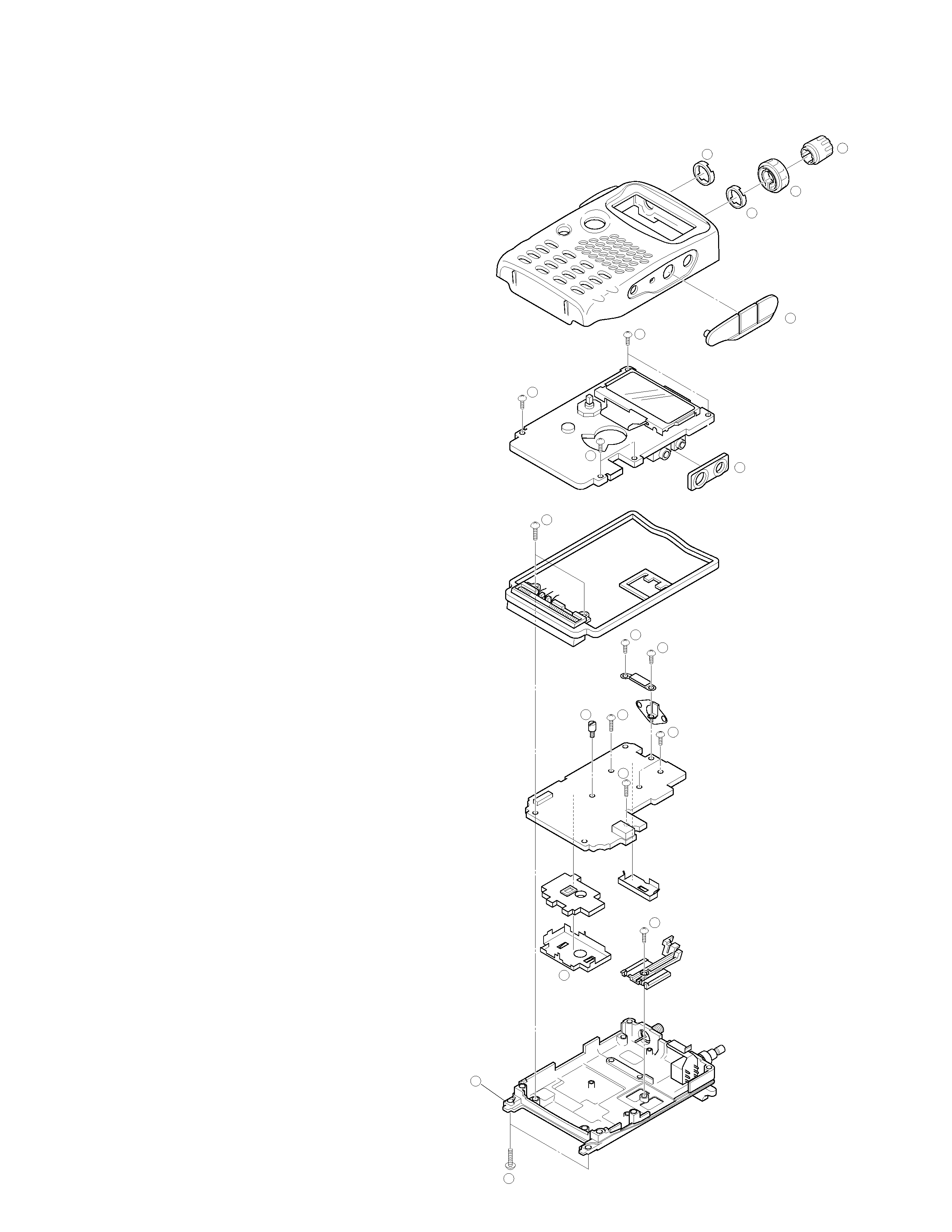
KNOB(ENC)
(K29-5159-03)
WHIP ANTENNA
(T90-0781-05):K
(T90-0789-05):T,E
KNOB(VOL)
(K29-5150-03)
CABINET ASSY
(A02-3620-13):T,E
(A02-3719-13):K
CAP
(B09-0615-23)
FRONT GLASS
(B10-2685-13):T,E
(B10-2723-13):K
KEY TOP
(K29-9107-12)
KNOB(PTT/MONI)
(K29-9108-13)
TH-F6A/F7E
2
DISASSEMBLY FOR REPAIR
1. How to remove the case assembly from
the chassis:
1. Remove 2 screws (1).
2. Remove 2 knobs (2) and 2 round nuts (3).
3. Remove the SP/MIC jack cover (4).
4. Open the bottom part of case assembly and lift the front
panel from the chassis (5).
2. How to remove the main PCB:
2-1. Control section
1. Remove the SP/MIC jack cover (6).
2. Remove 5 screws (7) and lift and remove the control PCB
(TX-RX A/3).
3. Extract the encoder flat cable from the connector.
2-2. RF section
4. Remove 8 screws (8), and 1 round screw (9), then remove
the RF shield cover. Remove the soldering that connects
the whip antenna and bar-antenna (3 locations).
5. Remove the battery terminal screw (0).
6. Lift and remove the RF PCB (TX-RX B/3).
2-3. PLL/VCO section
7. Remove the soldering (8 locations) that holds the PLL/VCO
shield cover (!) then lift the shield cover.
8. Lift the PLL/VCO PCB upward to seperate it from the main
PCB.
3
3
1
2
2
4
6
7
7
7
8
8
8
8
8
8
9
10
5
11
Fig. 1
TH-F6A/F7E
3
DISASSEMBLY FOR REPAIR
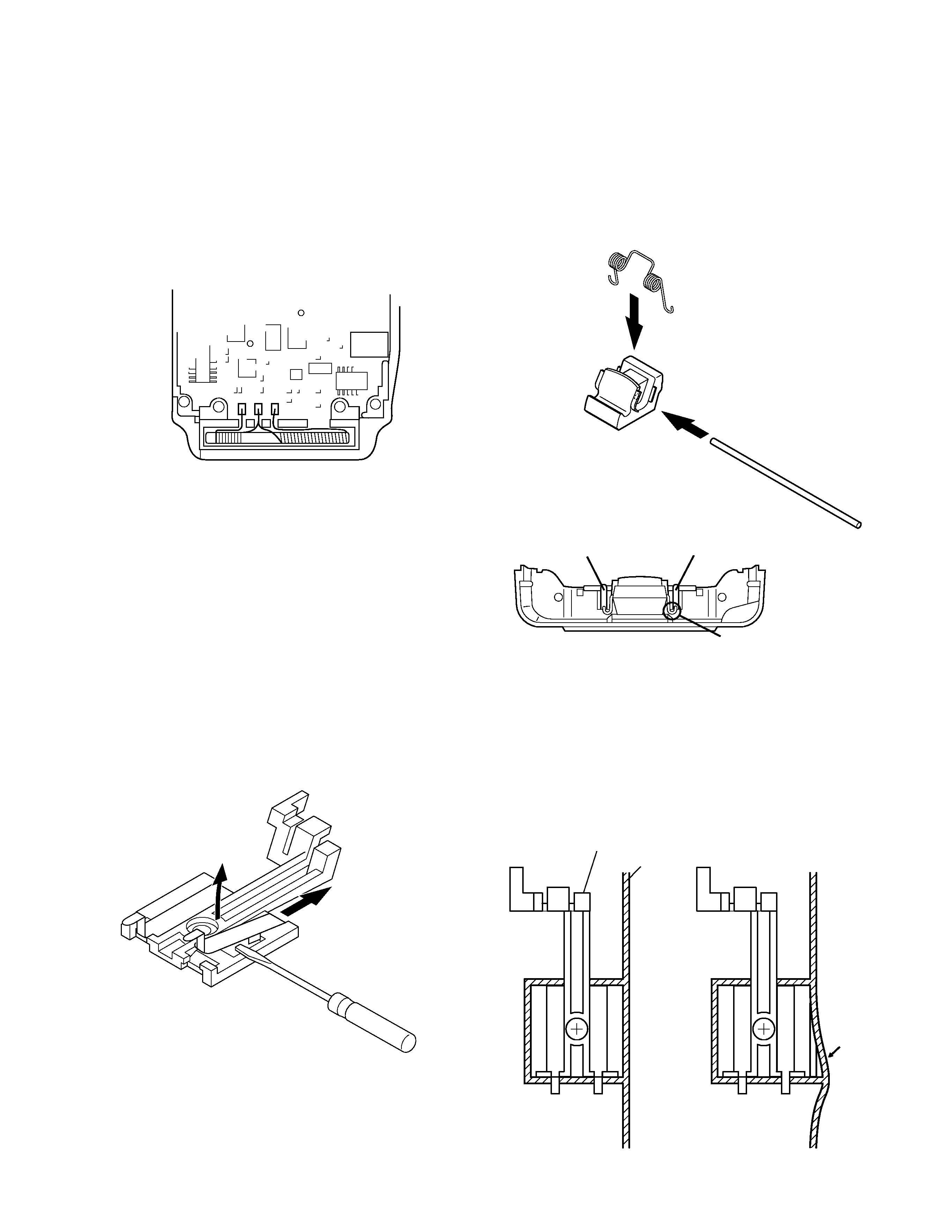
3. Soldering the Bar antenna wires
Before solding the bar antenna wires, form the wires as
shown in the figure 2.
Then solder the wires to lands on the PCB.
Fig. 2
4. Removing a relay terminal
Insert a screw driver between the relay terminal and its
holder.
Then pull the relay terminal as shown in the figure 3.
5. Assembling a release latch
Place a coil spring(1) on the release latch(2) as shown in
the figure 4.
Then insert a shaft(3) into the release latch.
Push the above assembly into the rear panel while the
end of coil spring is hooked to the "A" tab.
Fig. 4
2
1
3
Notch
Notch
A
6. Caution at the time of reassembling
While you are reassembling the battery terminal holder
(J19-5428) and the packing (G53-1532), confirm that the
packing is reassembled at the condition that any swell is
not occurred on it. If the packing is assembled with any
swell, width of body also becomes expansive.
J19-5428
G53-1532
Swell not
allowed
Fig. 3
Fig. 5
TH-F6A/F7E
4
CIRCUIT DESCRIPTION
1. A band receiver system
1-1. Receiver circuit
The A band can receive signals in two bands: VHF (220 MHz
band <K type only>) and UHF (K type: three bands). It uses
FM receive mode only, and uses double conversion with the
first IF of 59.85 MHz and the second IF of 450 kHz.
The first amplifier is divided into two bands: 137 MHz -
173.995 MHz (216 MHz - 260 MHz <K type only>) and 410 MHz
- 470 MHz. The incoming signal from the antenna passes
through a low-pass filter and a duplexer, and goes to an
independent amplifier (Q63, Q62) for each band.
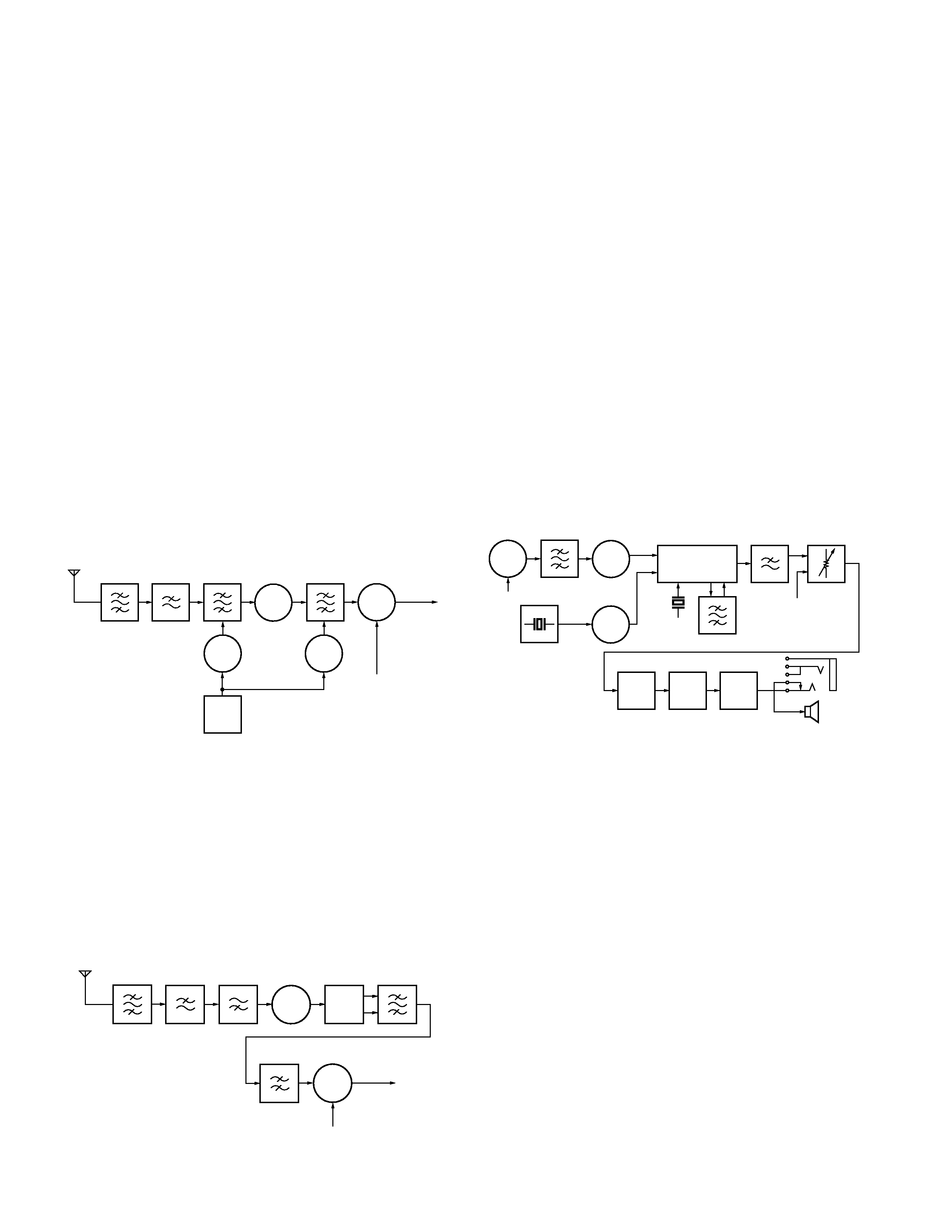
1-1-1. VHF band frontend
The incoming signal from the antenna passes through a
VHF band low-pass filter and a duplexer, passes through a
band-pass filter where it is tuned with varicaps (D76, D77),
and goes to the first amplifier (Q63). Unwanted signal
components are eliminated by a two-pole band-pass filter
where it is tuned by varicaps (D72, D75, D81, D83), and the
signal goes to the common mixer (Q45) for the A band. (K
type only: For 200MHz band reception, D74 is turned off with
a control signal to improve band-pass filter coupling and
ensure pass bandwidth.)
ANT
Q45
MT6C
04AE
BPF
APC&VTUNEA
MIX
Q63
3SK320
RFAMP
BPF
BPF
MPU
D76
D77
D72,D75
D81,D83
LPF
LO
1st IF
59.85MHz
Fig.1
1-1-2. UHF band frontend
The incoming signal from the antenna passes through a
UHF band low-pass filter and enters the first amplifier (Q62)
common to both A and B bands. The amplified signal is
distributed by L distributors (L95, L96) and goes to the LC filter
module (L92). Unwanted signal components are eliminated
by the filter, and the resulting signal passes through another
band-pass filter and enters the mixer (Q45).
ANT
BPF
Q62
3SK320
RFAMP
L95
L96
HPF
LPF
L92
Q45
MT6C
04AE
MIX
LO
1st IF
59.85MHz
BPF
LC FILTER
MODULE
1-1-3. Circuits following IF
The signal heterodowned to the first IF of 59.85 MHz by the
mixer (Q45) passes through a 15kHz MCF (XF2) and unwanted
signal components are eliminated. The resulting signal is
amplified by the IF amplifier (Q43) and goes to the FM IC (IC7).
The FM IC heterodowns it to the second IF of 450 kHz. Then,
the signal passes through a 15kHz external ceramic filter (CF4)
and goes to the FM IC again. The signal amplified by the IF
amplifier built into the IC is demodulated by the quadrature
FM demodulation circuit using a discriminator (CD1) and
converted into an audio signal and output.
The FM modulation signal output from the FM IC passes
through a low-pass filter consisting of a resistor and a capacitor
and is output to the control section. The demodulation signal
input to the control section goes to the electronic volume
(IC706, pin 13) to adjust the audio balance with the B band.
The output signal is amplified by the operational amplifier
(IC717), passes through an active filter consisting of Q719 and
Q717, and goes to the audio amplifier (IC707). The signal
amplified to a higher power by the audio amplifier becomes
the final output signal from the set and output through the
internal speaker or speaker output pin (J701).
Q45
MT6C
04AE
MIX
LO
X3
IC7
XF2
X1
TCXO
Q44
2SC
4915
IFAMP
MCF
Q43
2SC
5108(Y)
19.8MHZ
CF4
4.50KHz
LPF
IC700
VR
BAF
IC707
Q719
Q717
AUDIO
AMP
DE EMPHASIS
IC717
AMP
SP
J701
Fig.3
Fig.2
1-2. Mixer local oscillator
1-2-1. First mixer
The local oscillator signal for the first mixer is supplied from
the VCO-PLL circuit.
1-2-2. Second mixer
The local oscillator signal for the second mixer is a 59.4
MHz signal that is produced by multiplying the 19.8MHz TCXO
(X1) oscillator output with a multiplier (Q44).
2. B band receiver system
2-1. Receiver circuit
The B band has a broadband receiver circuit configuration
and implements broadband reception of 100 kHz to 1.3 GHz.
FM/AM/SSB/CW reception is possible in the range 100 kHz to
29.7 MHz, and FM/wide FM/AM/SSB/CW reception is possible
in the range 29.7 MHz to 1.3 GHz. The FM/AM receiver circuit
uses double conversion with the first IF of 57.6 MHz and the
second IF of 450 kHz. The SSB/CW receiver circuit uses triple
conversion with the first IF of 57.6 MHz and the second IF of
450 kHz. The wide FM receiver circuit uses single conversion
with the IF of 10.8 MHz.
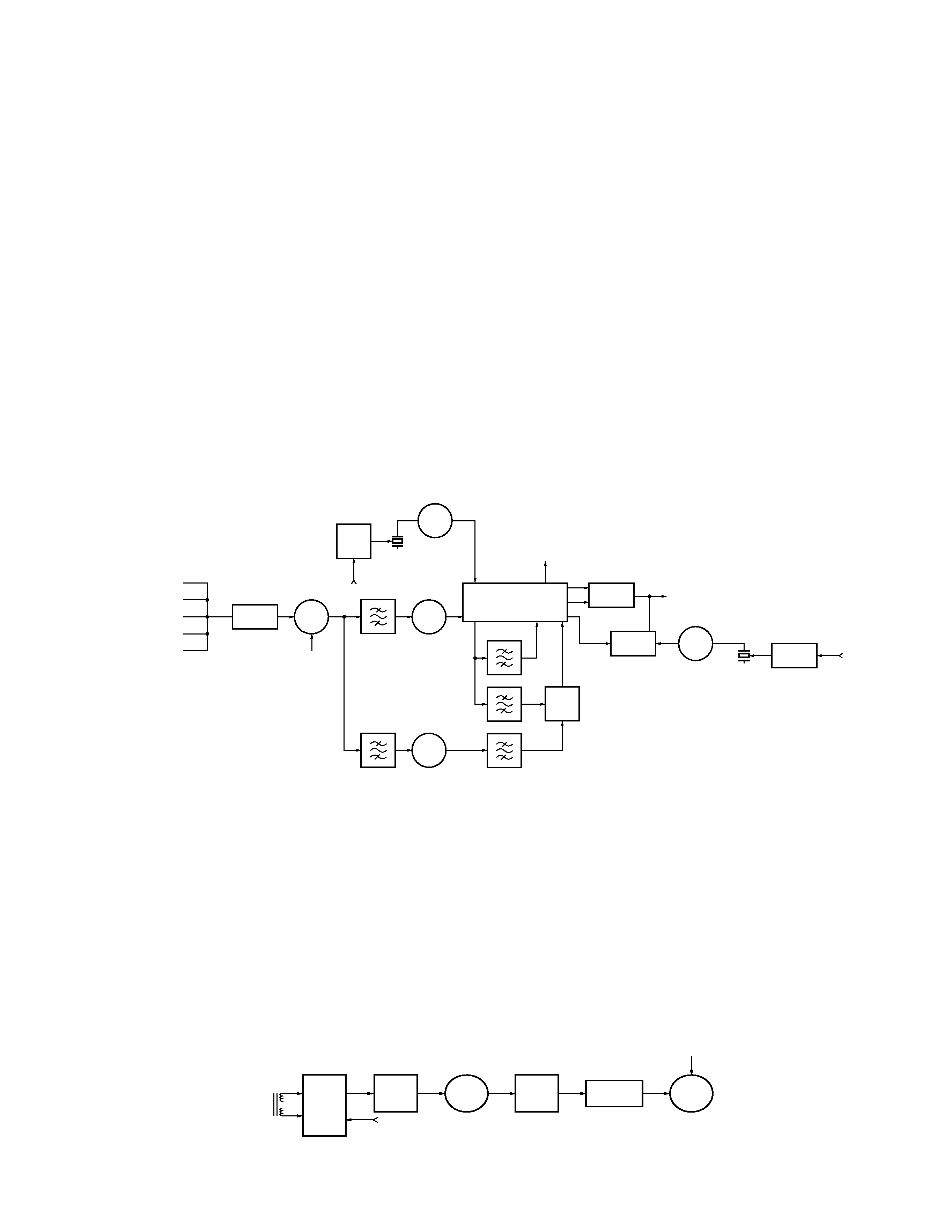
TH-F6A/F7E
5
CIRCUIT DESCRIPTION
Fig.4
The first amplifier is divided into four bands: 100 kHz - 50
MHz, 50MHz - 108MHz, 108 MHz - 265 MHz, 265 MHz - 600
MHz, and 600 MHz - 1.3 GHz. The incoming signal from the
antenna passes through a low-pass filter and a duplexer, and
goes to an independent amplifier for each band. Then, the
signal goes to the second common broadband amplifier (IC10)
and its output is fed to the mixer (Q28) and heterodowned to
the first IF.
2-1-1. FM/AM receiver circuit
The signal heterodowned to the first IF of 57.6MHz passes
through a 15kHz MCF (XF1), and unwanted signal components
are eliminated. The resulting signal is amplified by the IF
amplifier (Q26) and goes to the FM IC (IC5). The FM IC
heterodowns it to the second IF of 450 kHz. In FM mode, the
signal passes through a 12.0kHz external ceramic filter (CF3)
and goes to the FM IC. The signal amplified by the internal IF
amplifier is demodulated by the quadrature FM demodulation
circuit using a coil (L19) and converted into an audio signal
and output. In AM mode, the signal passes through a 4kHz
external ceramic filter CF1 and goes back to the FM IC. It is
amplified by the AM AGC amplifier built in the FM IC, an audio
output from the FM IC as an audio signal.
2-1-4. AM bar antenna receiver circuit
This unit incorporates an AM bar antenna, and either the
bar antenna or the supplied antenna can be selected in the
520kHz-1.8MHz (SW) and 3.5MHz-10.1MHz (MW) bands (the
initial value: bar antenna). The bar antenna has two kinds of
tuners for SW and MW tuning, one of which is selected with a
switching FET (Q32, Q48, Q52). The antenna is tuned with a
varicap (D60) for AM tuning to select a desired signal. The
signal from the bar antenna is amplified by and its impedance
is converted by the buffer amplifier (Q59), and the resulting
signal goes to the common mixer (Q28) for the B band. The
signal is routed over the same path for AM demodulation as
for the supplied antenna after leaving the mixer.
19.05MHZ
FINE2
D20,24
KV1566J
TUNE
IC4
TA4101F
SSB DET
SSB/CW
Q22,29
UPA672T
IC5
TK10931V
SW
FM
AM
SMB
SQB
Q23
LMX
2N
OSCILLATOR
453KHz
SW
CF1
450KHz
CF3
CF2
10.8MHz
D25
DAN
235E
TUNE
D29
HVC
376B
Q27
2SC
4915
OSCILLATOR
Q26
2SC
4915
IF AMP
Q28
MT6C
03AE
MIX
FINE1
UHF(600~1300)
UHF(265~600)
VHF(108~265)
HF
HF
IC10
MPC2746TB
AMP
LO
57.6MHz
XF1
10.8MHz
MCF
Q24
2SC
4915
CF5
Q28
MT6C
03AE
SW
IC10
MPC2746TB
AMP
D57
HSC277
TUNE
D60
KV1566J
SW
BAR
ANT
Q6,Q4
Q48,52
2SK1824
Q32
2SK1830
MIX
LO
Q59
3SK320
RF AMP
Fig.5
2-1-5. Audio signal
The FM and AM demodulation signals output from the FM
IC (IC5) pass through a low-pass filter consisting of a resistor
and a capacitor, and goes to the switching FET (Q29), from
which a switched signal is output to the control unit. The
SSB/CW demodulation signal passes through an RC LPF,
connects to the Q29 output section, and output to the control
unit through a line common to all modes. The demodulation
signal input to the control unit goes to the electronic volume
(IC706, pin 16), the audio balance output with the A band is
restricted, then the signal is output. It joins the A band
demodulation signal and is processed in the same manner
for both A and B bands.
signal demodulated by the diode detection circuit is output.
2-1-2. SSB/CW receiver circuit
In SSB/CW mode reception, the signal takes the same path
to CF1 as in AM mode. The signal input to the FM IC again is
amplified by the AM AGC amplifier in the FM IC, then output
from the AM IF output pin. The signal is fed to the third mixer
(IC4) and converted to an audio signal and output.
2-1-3. Wide FM receiver circuit
The signal converted to the first IF of 10.8 MHz passes
through a ceramic filter CF5 for wide FM, and is amplified by
the IF amplifier (Q24). The signal passes through ceramic filter
CF2 again to eliminate unwanted signal components, and goes
to the FM IF input (pin 7) of the FM IC. The input signal is
amplified by the IF amplifier in the IC, demodulated by the
quadrature FM demodulation circuit using an L18 coil, and
