LCD COLOR MONITOR
KVX-5-L/-S
SERVICE MANUAL
© 2001-7 PRINTED IN KOREA
B51-5743-00 (K/K) 1979
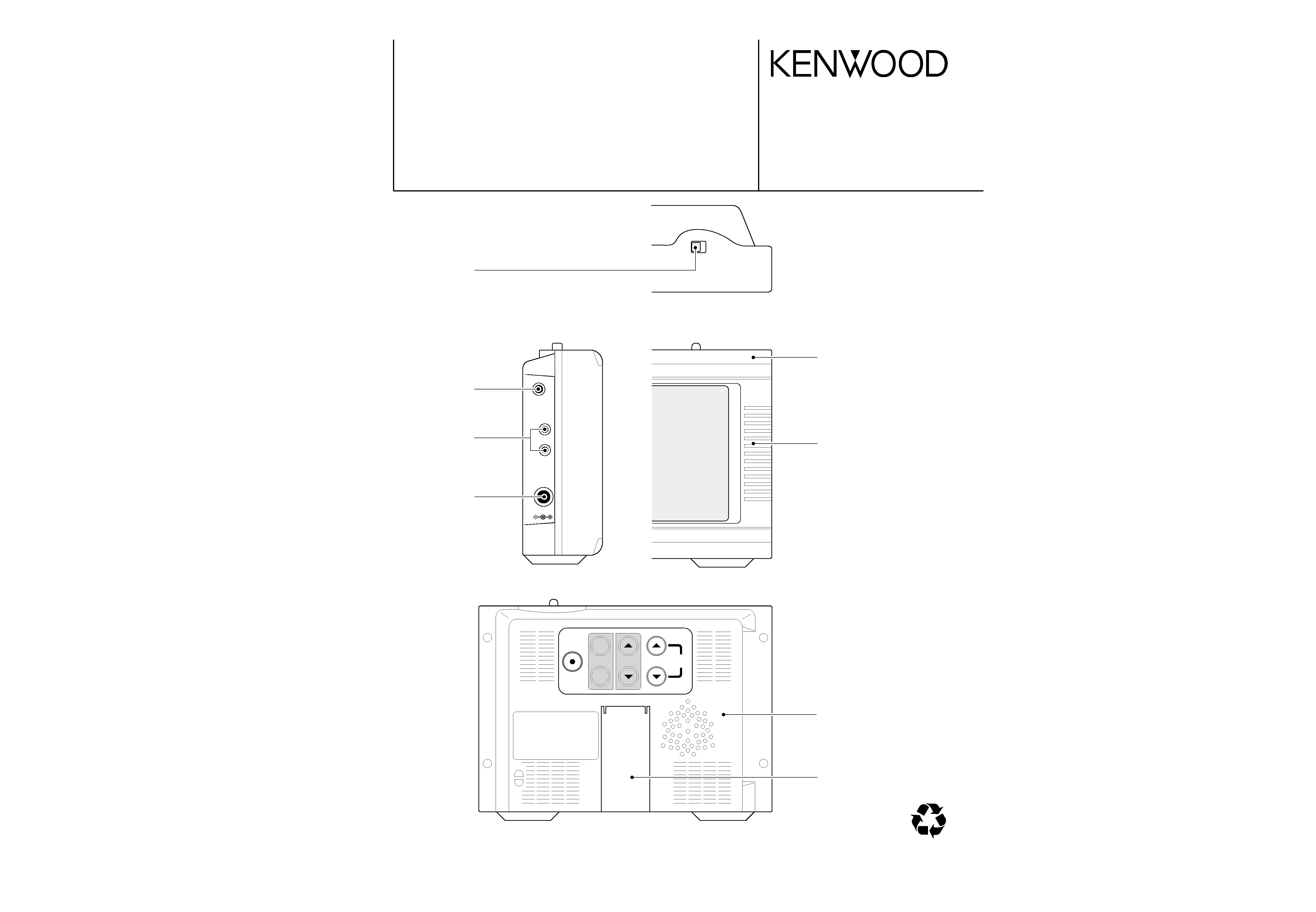
MENU
VOL.
INPUT
BRIGHT
MENU
SET
POWER
OFF
ON
TFT ACTIVE MATRIX
PHONES
AV1 IN
AV2 IN
DC IN
AV1
AV2
Connector
(E11-0947-08)
Connector
(E11-0949-08)
Decoration
(B02-0083-08): L
(B02-0084-08): S
Front panel
(A60-2167-08)
Power knob
(K29-8097-08): L
(K29-8098-08): S
DC jack
(E03-0386-08)
Rear panel
(A80-4153-08)
Stand
(A09-1245-08)
70%
L: Blue, S: Silver

AV cable (1)
AC adaptor (1)
(W08-0687-08): T
(W08-0688-08): E
(E30-7241-08)
(J39-1039-08)
Cushion (2)
Action to be taken
Check the AC adaptor for proper connection.
Check that the POWER switch is turned on.
Check that the brightness and volume are
minimized or the system is put in mute state.
Check the selected A V input (AV1 or AV2) for
connection to A V equipment.
Check for reception of audio/video signals fr om AV
equipment.
Check the brightness for maximum or minimum.
Check the sound volume for minimum or check
the system for being put in mute state.
Check headphones for being plugged into the
system.
Check for reception of radio interference from
other equipment, etc. (T urn of f the power of other
equipment.)
Check COLOR, TINT, and PICTURE for proper
adjustment.
Check the direction of the crystal liquid panel for
proper adjustment.
Check the brightness for proper adjustment.
When the temperatur e of the system is low , the
screen becomes darker than usual just after the
power is turned on because of the characteristic of
the liquid cr ystal panel. W ait for a while until the
temperature goes up. The screen will get light as
usual.
Problem
No image and no sound
No image and no sound ( NO
SIGNAL appears)
No image, or black or white
screen
No Sound
Poor-quality image displayed
Image doubly displayed
Image fading
Image swaying
Stripes and patterns
Inappropriate
color or light color
Dark screen
Dark screen in the initial stage
Troubleshooting Problems
If the system does not work as you expect, perform the following checks before contacting
Customer Support.
If this product interferes with radio reception during use, place it far enough away from the
radio to eliminate the interference.
·
·
·
·
·
·
·
·
·
·
·
·
·
·
·
·
·
·
KVX-5-L/-S
2
CONTENTS / ACCESSORIES
CONTENTS / ACCESSORIES ...................................2
DISASSEMBLY FOR REPAIR....................................3
ADJUSTMENT ............................................................4
PC BOARD .................................................................5
SCHEMATIC DIAGRAM .............................................7
EXPLODED VIEW ......................................................9
PARTS LIST..............................................................10
PARTS DESCRIPTIONS ..........................................13
SPECIFICATIONS .......................................Back cover
Contents
Accessories

1
1
1
2
2
3
4
4
4
4
4
3
3
3
1 x2
x2
4 x2
PV04
PM01
P502
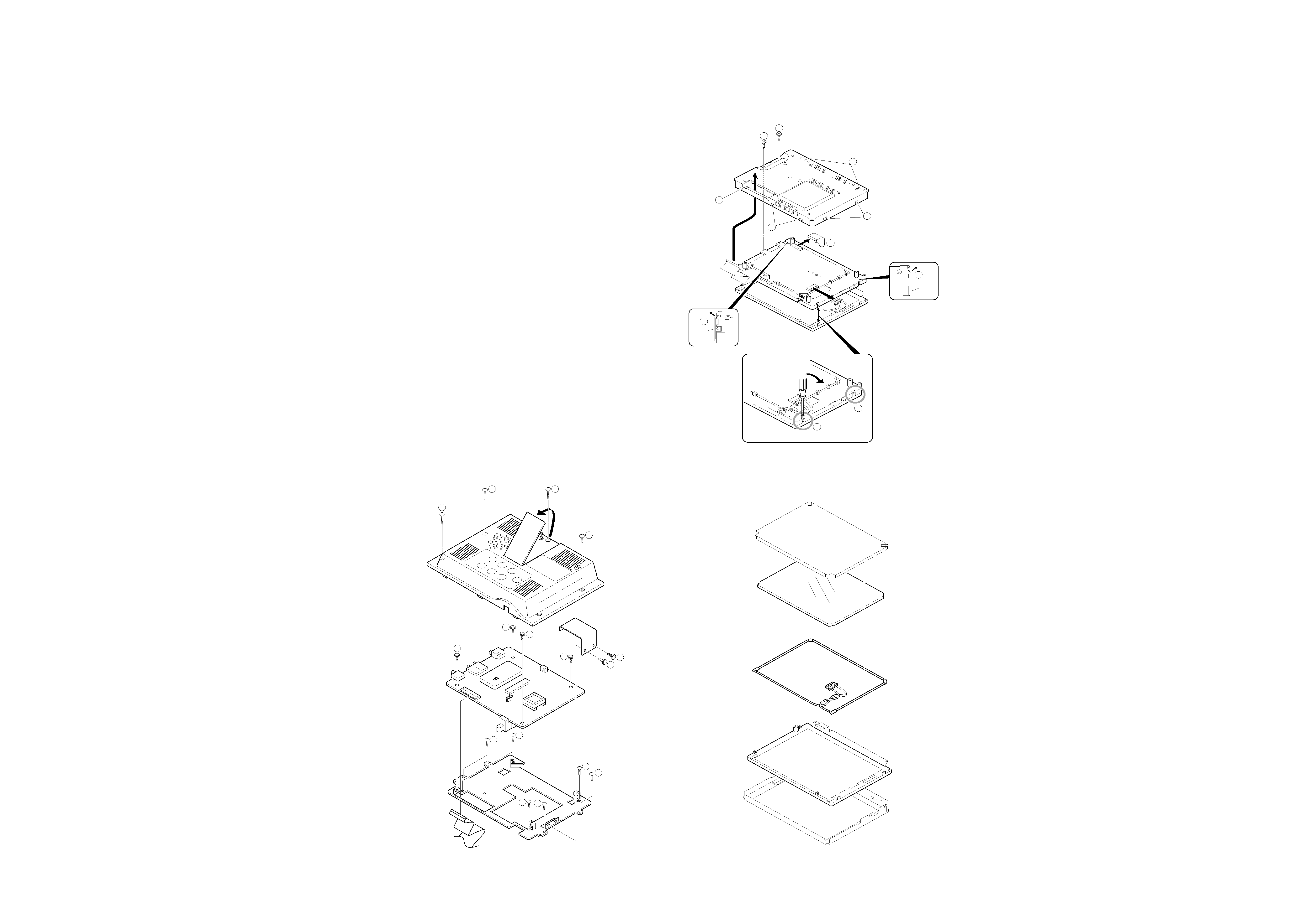
How to Replace the Backlight
1. Remove screws (
1X5) and rear panel.
2. Disconnect a speaker connector(P502) and flexible
cable(PM01).
3. Remove screws(
2X2)and a metal.
4. To remove a PC board, remove a flexible cable (PV04)
and screws(
3X4).
5. Remove screws(
4X8)and a metal.
6. To remove a shield cover A, remove screws(
5X2)and
then release hooks(
6X7) using a flat screw driver and
so on.
7. To remove a PC board, disconnect a connector(CN3)
and a flexible(
7).
8. Release hooks (
8X2) and then remove shield cover B.
9. Release hooks(
9X2)using a flat screw driver and so on,
then remove a LCD.
10. Remove a backlight.
5
5
6
SHIELD COVER A
CN3
CN3
6
6
8
7
9
9
6
x1
8 x1
SHIELD
COVER B
SHIELD
COVER B
BACK LIGHT
LCD
SHIELD COVER B
KVX-5-L/-S
3
DISASSEMBLY FOR REPAIR

ADJUSTMENT
ITEMS
ALIGNMENT
POINT
SIGNAL
INPUT
SETTING
OUTPUT SETTING
ALIGN. FOR
Fig
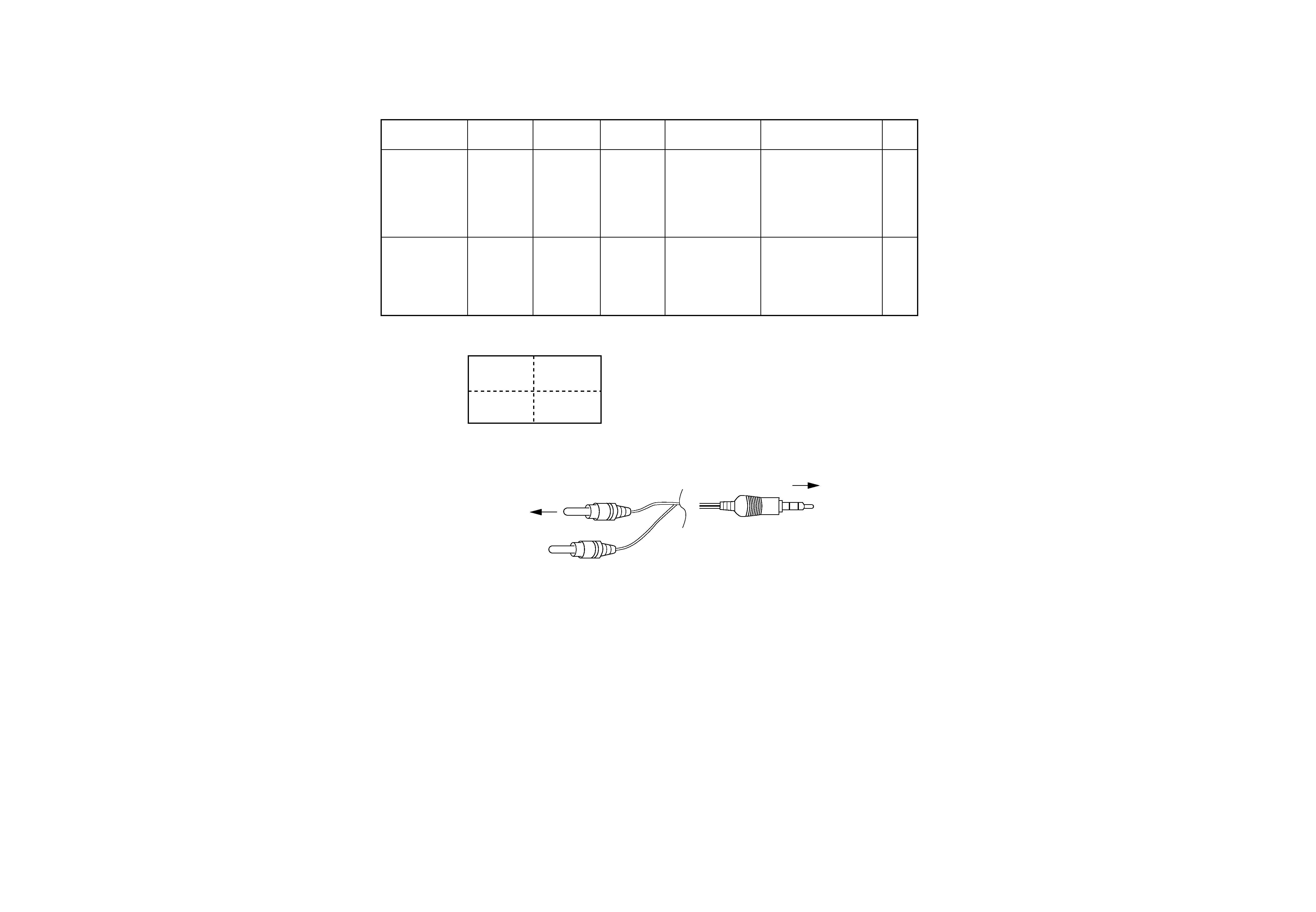
1. OSD POSITION
ADJ.
LM01
CENTER
CROSS
(Color Pattern
Generator)
AV IN
-
· To indicate "MUTE "in
the LCD, press down vol.
UP and DOWN keys
simultaneously.
· Set the "MUTE " in the
middle of the LCD.
Fig. 1
2. AUDIO OUTPUT
ADJ.
RS08
1kHz
AV IN
Input level
1Vp-p
(4.7k
terminate)
Connect a
oscilloscope to SP
connector (PS02)
with 8 load.
Adjust audio output
become to 0.6 ± 0.05Vp-p
at Vol. "50".
Fig. 2
MU TE
Fig. 1
Fig. 2
TO AG
AUDIO
VIDEO
KVX-5(AV IN)
KVX-5-L/-S
4
ADJUSTMENT

RP34
RP35
CP40
RP33
5
1
CP04
CP39
RP04
RP03
CP17
RP37
RP22
RP23
CP22
CP41
CP32
CP43
CP23
1
3
R
V18
R
V13
CV10
CV12
R
V17
CV13
R
V20
CV17
R
V22
CV19
CP36
RP19
RP20
CV27
LV03
CV24
RV29
CP42
RV28
RV31
R
V34
CV26
RV30
RM33
RM34
CV28
CV29
CV30
R
V35
CV31
RM32
RM35
CM29
RM31
RM48
RM29
RM25
RM28
RM49
RM47
RM24
RM46
CM04
4
1
1
3
RM23
CM22
CP20
RM39
RP17
RP21
8
5
RM38
CM14
RP25
CP38
RM12
RM17
RM42
RM18
RM11
RM19
RM16
RM56
RM54
CP29
RM52
CM35
RM21
RM55
CP31
RM22
CM19
CM18
RM20
RP12
1
5
CV53
CV65
CV63
R
V83
R
V97
RS06
RS09
CS09
RS07
CS11
R
V69
RS01
RS02
RM10
RM43
CM11
CM33
CM09
CM32
R
V103
R
V102
CM10
CV40
CM30
CV41
CV33
CM31
CM05
CV74
41
RV48
RV47
7
1
R
V51
8
5
8
14
R
V63
CM06
CV45
4
1
CV75
CV76
R
V104
R
V105
R
V49
CV43
CV73
L
V01
CV36
CV35
CV32
R
V36
CV34
8
5
CV37
R
V04
CV38
R
V33
R
V92
R
V05
RV
1
1
R
V07
R
V06
R
V81
R
V89
BE
BE
BE
BE
R
V23
CV20
R
V19
R
V59
RV27
R
V86
CV46
R
V65
R
V67
CV47
R
V55
CV22
R
V99
CV09
CV50
RV57
RS11
RS10
RP01
CP03
DME
KW E T
DP03
DP07
QP13
ZP06
ZP05
SP01
POWER
OFF
ON
DP12
DP09
QP06
DP08
ZP04
DP10
DP1
1
QP12
ZP02
QP05
QV10
QV11
QV23
QV22
QV21
QV06
QV16
DP02
DP01
+
RP39
CP05
RP32
RP36
B
E
B
E
CP02
RP27
RP26
RP31
1
RP38
11
CP25
R
V16
R
V14
CV16
R
V15
CV11
CV15
CV18
42
2
1
R
V12
R
V08
R
V09
R
V10
8
9
CP33
CP37
1
TP01
R
V32
8
6
16
1
7
4
XV03
5
8
1
15
28
10
11
5
20
1
RM26
CP34
CP24
CP18
LM01
RM27
RM37
RP16
9
16
8
RM36
RM15
RM40
CP35
RM14
RM41
1
7
8
TL03
RM13
RM06
CP30
RP05
RM58
1
14
CP1
1
CM01
CP14
CP16
LP03
1
CP15
RP14
RP15
RP13
CP13
PS02
CP01
CS64
1
8
3
8
1
3
1
16
RS08
9
CV61
R
V84
CV62
CS05
4
5
CS12
R
V96
1
14
TL04
TL05
CV48
XM01
R
V50
CV42
R
V52
TL06
TL01
CV08
CV44
CV66
R
V37
R
V40
R
V45
21
RV91
R
V64
RV93
R
V58
B
E
B
E
B
E
B
E
B
E
R
V53
RV88
R
V46
RV90
RV85
22
XV02
RV87
CV23
24
RV26
2
XV04
1
23
CV72
R
V98
6
2
1
R
V62
3
4
CV14
2
6
CS13
3
4
CS02
1
2
3
FP01
LP02
KW E T
DME
PWMA026
O
O
I
I
G
G
DP05
QP02
QP10
QV07
QM05
QM04
ZP03
QM02
QP1
1
QP09
QM03
DP06
QV17
QS01
QM06
QV24
PP01
PV02
PV01
PS03
A
V
IN1
HEADPHONE
DC
IN
A
V
IN2
PV04
QM01
PM01
QV25
QV26
QV27
QV01
QV05
DP04
ACE
G
I
BD
F
H
J
2
1
3
5
7
4
6
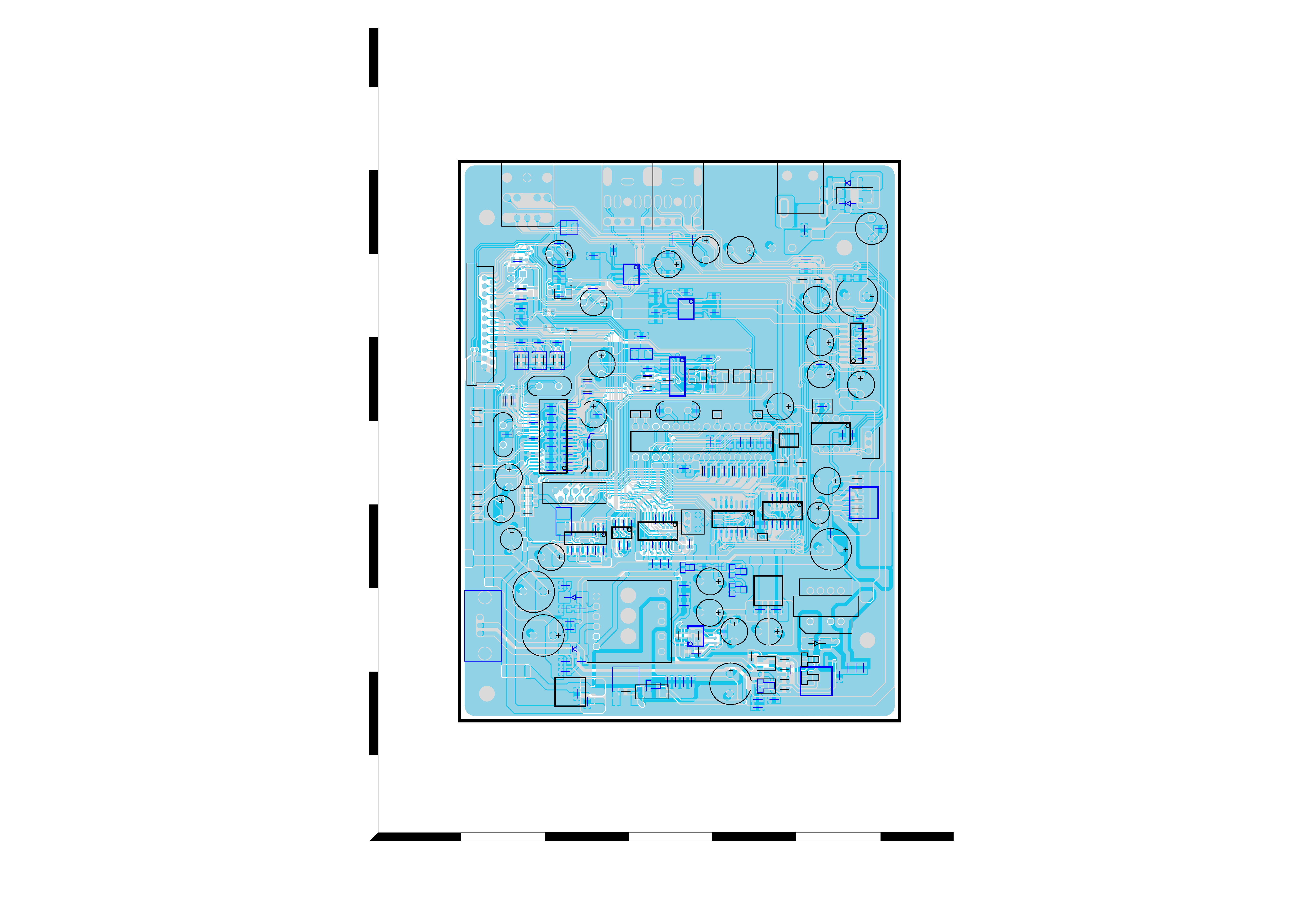
Refer to the schematic diagram for the value of resistors and capacitors.
PC BOARD (Component side view)
5
6
