© 2004-5 PRINTED IN JAPAN
B53-0171-00 (N) 2703
DVD PLAYER
KDV-S210P/S220P
/S230P/S240P
SERVICE MANUAL
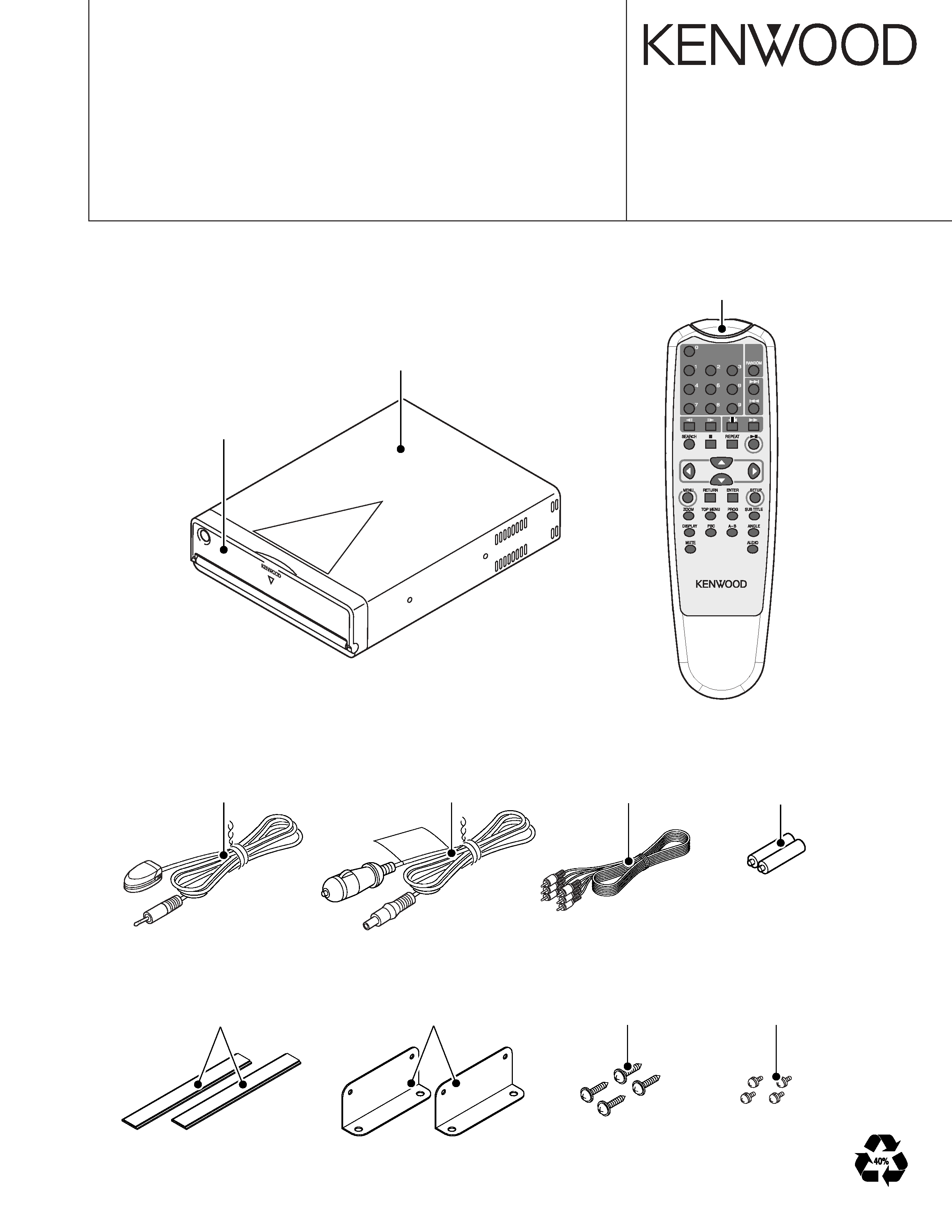
Size AAA battery
(Not supplied)
Remote controller assy
(A70-2066-08)
Panel assy
(A64-3526-08): KDV-S210P
(A64-3528-08): KDV-S220P
(A64-3529-08): KDV-S230P
(A64-3530-08): KDV-S240P
Tapping screw
(N09-6274-08) x4
Magic tape
(H30-0514-05) x2
Remote control sensor assy (6m)
(T95-0264-08)
Mounting hardware
(J22-0237-08) x2
Metallic cabinet
(A01-2845-08)
Cord with DC plug (2.4m)
(E03-0405-08)
Cord with pinplug (3m)
(E30-6389-08)
SEMS
(N09-6273-08) x4
RC-DV500
Except KDV-S210P
2
KD
V
-S210P/S220P
/S230P/S240P
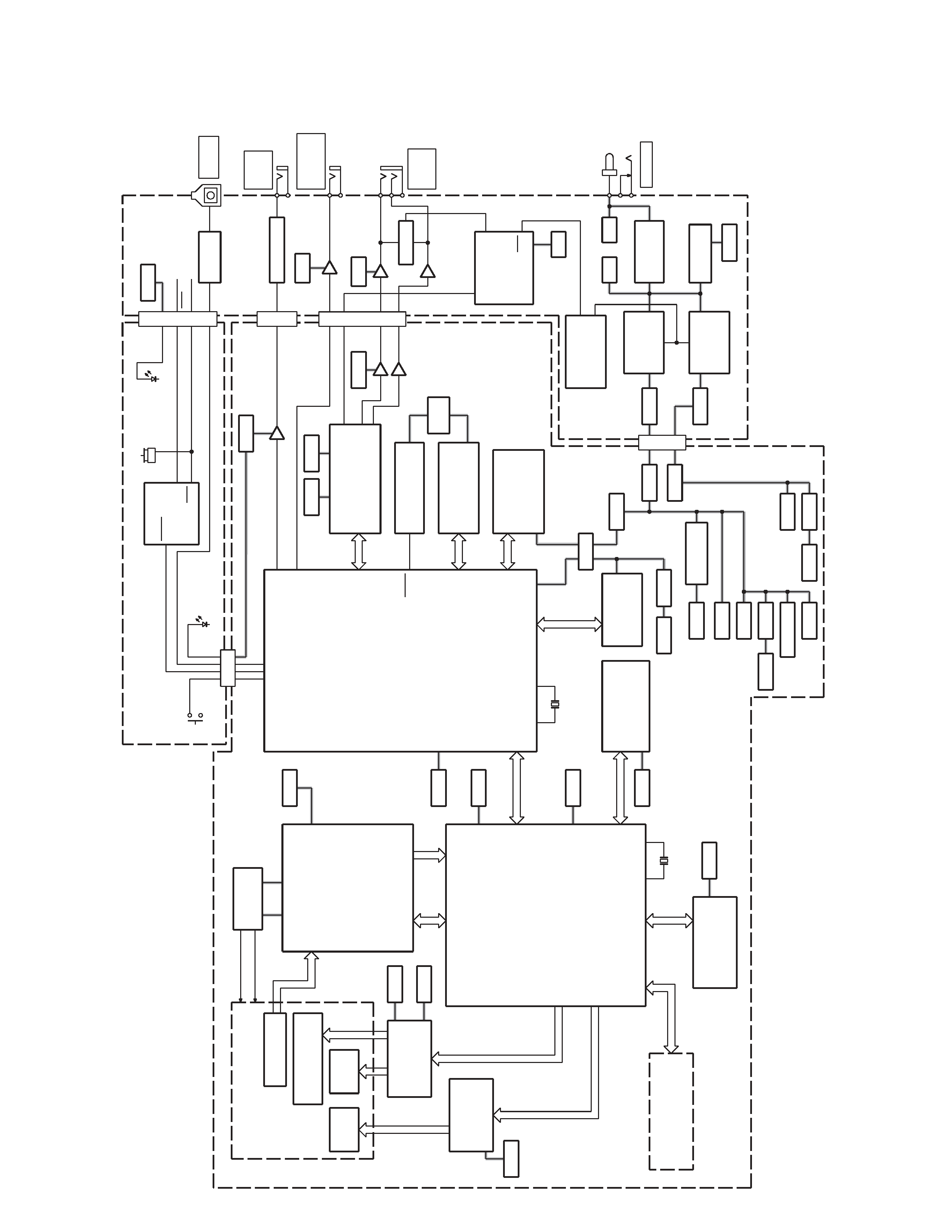
BLOCK
DIA
GRAM
PROCESSOR
-DIGITAL SERVO CONTROL
DVD/CD DATA DECODING
SU6
SU1
SU3
MOTOR DRIVER
PWM
SU2
BTL
MOTOR DRIVER
HEAD AMPLIFIER
-GENERATING SERVO
-AUTO GAIN CONTROLLING
S+7V
MMVC
MVCC
DECODING & CORRECTING
-F/E CONTROL uP
-DATA BUFFERING
SVCC
-F/E PROGRAMING
FLASH MEMORY
3.3V
RFVCC
3.3V
VCC27
RFVCC
-DATA BUFFERING
DVD MPEG DECODING PROCESSOR
-MPEG DECODING
-B/E & SYSTEM CONTROL uP
U1
SU7
-B/E FRAME
SDRAM
-DVD/CD DATA
U34
CIRCUIT
LASER DRIVE
SQ4,5
U3
-F/E FRAME BUFFER
SDRAM 1Mx16BITS
-WORKING MEMORY
ACTUATOR &
BRUSHLESS
SY1
-F/E SYSTEM CLOCK
33.8688MHz
CERAMIC RESONATOR
CODE STORED
128kx8
-B/E SYSTEM CLOCK
CRYSTAL RESONATOR
27MHz
Y1
VCC27
-INCLUDING OVER
2ch AUDIO DAC
U35
DIGITAL FILTER
SAMPLING
U9
-RESETING
RESET IC
for U1
STORED
-SETUP & RESUME
EEPROM
INFORMATION
U2
U28
CODE STORED
-B/E PROGRAMING
FLASH ROM
VCC33
Q1
MMVC
MVCC
SVCC
3.3V
RFVCC
VCC33
AVCC
AVCC
RESET VCC
VCCA
S+7V
U5
REGULATOR
3.3V FIXED
SQ3
+7V
S7V
VCC
VCC
+7V
U23-1
U23-2
BUFFER
U27
POST LPF
-2nd ORDER
ACTIVE LPFx2
3.3V
CB5
CBP5
CBP7
CB7
CB502
CBP502
CB3
CBD3
1MBITx8
BUFFER
4Mx16BITS
SERVO SIGNAL
RF AMPLITUDE
ERROR SIGNALS
INSERTION
DISC
SLIT
INDICATOR
EJECT SW
UD3
NAND GATES
POWER SW
INDICATOR
POWER
CBD1
CBP1
VCC
S7V
UP1
REGULATOR
SWITCHING
REGULATOR
SWITCHING
UP2
+B1
REGULATOR
5V
QP30
REGULATOR
QP40
28V
CIRCUIT
BU VCC
-GENERATING
TIMING
ON/OFF SW
DELAY CIRCUIT
VCC
RESET
REDUCING +B1
CIRCUIT
MUTE
-SENDING
DRIVING
-MUTE TR
+B1
ACTIVE LPFx2
LPF
-2nd ORDER
UP3-2
UP3-1
S7V
MUTE TR
QP4,5
UP4
VCC
75 Ohm
VIDEO
DRIVER
TRP1
PULSE TRANS
BU VCC
EYE INPUT
REMOTE
DC INPUT
ANALOG
OUT
AUDIO
VIDEO
OUT
COMPOSITE
DIGITAL
OUT
AUDIO
REMOTE
EYE
SPINDLE
MOTOR
to
SLEDGE
MOTOR
to
PICKUP HEAD
from SENSOR of
ACTUATOR COIL of
PICKUP HEAD
to
to CD LD
to DVD LD
+B
ERROR SIGNAL
INPUT
RF & SERVO
I/O
VPA
VM
PVCC
VCC
INTERFACE
COMMAND
DSP
CDLD
DVDLD
DSP COMMAND
INTERFACE
SIGNAL INPUT
RF & SERVO
CONTROL
LOADING
MECHANISM
OUTPUT
SERVO DRIVE SIGNAL
INTERFACE
FLUSH MEMORY
INTERFACE
SDRAM
AVDD5
INTERFACE
ATAPI
VDD 3.3
INTERFACE
SDRAM
INTERFACE
ATAPI
FLUSH MEMORY
EEPROM
RESET
DIGITAL AUDIO
VC25
INTERFACE
INTERFACE
INTERFACE
SPDIF OUT
SPDIF
UDAC
VIDEO DAC OUT
VC33
VCC
OUTPUT
SIGNAL
ERROR
RF & SERVO
RESET
HARDWARE
for F/E
INCLUDING
A
UX4
A
UX2
A
UX7
VCC
VDD
VOUTR
VAA
VOUTL
VDD
ZRR
VCC
VCC
VCC
LED
RED
P DWN
P ON
+B DWN
LED
GREEN
IR
VSW
EN
VIN
VSW
EN
VIN
P ON
ZER
O
MUTE
VCC
V+
V+
CH-R
CH-L
VCC
+B DWN
P ON
IR
ZERO MUTE
SLOT-IN
LOADING MECHANISM
DISPLAY PCB
POWER & OUTPUT PCB
COMBO PCB
TRAVERSE MECHANISM

3
KDV-S210P/S220P
/S230P/S240P
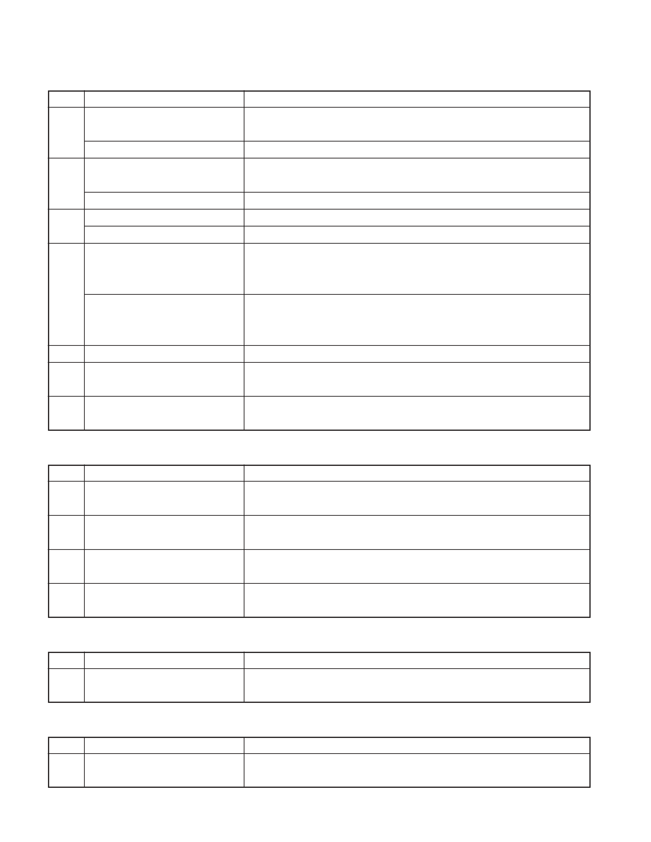
COMPONENTS DESCRIPTION
COMBO PCB
Ref. No.
Application / Function
Operation / Condition / Compatibility
MPEG decoding control
DVD MPEG images are decoded.
Dolby digital decoding control
Outputs of Dolby digital audio are decoded.
LPCM audio decoding control
LPCM audio of CD and DVD are decoded.
DVD navigation control
DVD navigation is controlled.
ATAPI communication control
ATAPI communication is control in order to control F/E.
U1
Built-in microcomputer for controlling
System as a whole and B/E are controlled. 32bit RISC microcomputer is built-in.
system and B/E system
Built-in video DAC
Video DAC is built-in to output current for composite video output from No. 106 pin.
Digital audio DAC control output
Audio signals are output from No. 32 (TWS), 33 (TSD0), 39 (MCLK), and 40 (TBCK) pins. Also,
DAC system control is conducted using No. 160 (AUX0), 161 (AUX1), and 168 (AUX6) pins.
Controls for keys and remote control
No. 162 pin is input for EJECT key. When receiving input, it is in L. No. 166 pin is for
remote control input. When receiving input, there will be pulse input.
U2
EEPROM for storing system setting
EEPROM for storing system setting information and resume information.
information and resume information
U3
Frame buffer memory
Decoding data buffer memory.
Program memory
Memory for program control.
U5
3.3V regulator
From No. 3 pin, VCC (5V) is input and from No. 2 pin, VCC33 (3.3V) is output.
U9
System reset control
Rising/Falling of VCC (5V) is detected by No. 5 pin, and L-reset output is made from No. 4 pin.
U23
For audio post LPF
CH1-side is Rch and CH2-side Lch. Constitutes a multiple feedback-type active LPF.
U27
SPDIF output, Pulse transformer driver
Inverters are connected in 3-step parallel connection for increased current capacity and
output to the pulse transformer.
U28
B/E program memory
Flash memory for storing B/E program memory.
U34
Program memory
Flash memory for storing programs.
Digital audio signal is input from No. 3 (TWS), 2 (TSD0), 16 (MCLK), and 1 (TBCK) pins.
U35
Digital audio 2ch DAC
Also, signals for DAC system control are input from No. 15 (AUX0), 14 (AUX1), and 13 (AUX6) pins.
Output for Lch analog audio is made from No. 7 pin and that for Rch is made from No. 8 pin.
DVD/CD digital servo control
Built-in DVD/CD digital servo equalizer and various timing generation circuit.
DVD/CD data decoding control
Data generation from RF of DVD/CD, error correction and control over scramble analysis
SU1
and release.
F/E section built-in system control
F/E section 8bit microcomputer for system control.
microcomputer
ATAPI communication control
ATAPI communication control with B/E.
Pickup actuator driver
Control signals for focus and tracking actuator signals of the pickup are received by No. 1 and
No. 26 pins respectively and currents are output from No. 13 and14 and No. 15 and 16 pins.
SU2
Feed motor driver
Control signals for the feed motor is received at No.6 pin and currents are output from
No. 11 and 12 pins.
Motor driver for slot loading mechanism
Control signals for slot loading mechanism motor is received at No. 23 pin and currents
are output from No. 18 and 17 pins.
4
KDV-S210P/S220P
/S230P/S240P
Ref. No.
Application / Function
Operation / Condition / Compatibility
Spindle motor driver
Timing is controlled by No. 18 pin control signal for the 3-phase brushless spindle motor, using
SU3
No. 1~6 pins Hall element input signals, while current outputs are made from No 20, 22 and 24 pins.
Spindle motor rotation detection
Rotation FG output for controlling spindle motor is output from No. 27 pin.
DVD/CD servo error signal replay
Generation of various servo signals from pick up signals.
SU6
amplifier control
Built-in DVD/CD laser APC circuit
Built-in LD current control circuit for DVD/CD.
SU7
Frame buffer memory
Memory for temporarily caching read data of DVD/CD.
System memory
External microcomputer memory for F/E system control.
CH1-side
CH1-side
Servo reference voltage generation
Signal after dividing VC25 (2.5V) into 2.1V enters the positive phase and output from the
SU8
amplifier
output terminal as buffer output.
CH2-side
CH2-side
RFRP (mirror detection signal)
RF bottom hold signal and its DC are input to reverse input and positive input respectively
generation amplifier
for canceling DC fluctuation. These then can be used as mirror signals.
SQ3
3.3V regulator
VCC (5V) is input from No. 3 pin and 3.3V is output from No. 2 pin.
SQ4
Driver for LD-driving for CD
CD's LD current control signals output from SU6 are received at base and the current
amount for LD driving is controlled.
SQ5
Driver for LD-driving for DVD
DVD's LD current control signals output from SU6 are received at base and the current
amount for LD driving is controlled.
THERMISTER PCB
Ref. No.
Application / Function
Operation / Condition / Compatibility
UT1
Inverter
Output from UT2 comparator is inverted. Input is made on No. 2 pin and output on No. 4
pin. Active L.
UT2
Comparator
Signal from thermister is inverse input and reference voltage is input to positive-phase
input. Output from thermister is comparated and output from No. 4 pin. Active H.
QT1
Switching TR
UT1 output is received on the base and output is inverted when it is made. The output is
feedback into the positive-phase input at UT2 for containing the fluctuations in outputs.
THT1
Temperature detection thermister for
Resistance value is low at low temperature and high at high temperature.
thermal shutdown
DISPLAY PCB
Ref. No.
Application / Function
Operation / Condition / Compatibility
UD3
Power supply ON/OFF delay circuit
With +B_DWN of reduced voltage detection circuit and OR of /P_ON signal, /P_DWN
NOR gate IC
signal is generated.
POWER & OUTPUT PCB
Ref. No.
Application / Function
Operation / Condition / Compatibility
UP1
VCC (+5V) generation switching
Power supply is input from No. 2 pin and switching output is made from No. 3 pin.
regulator IC
Going via choke coil, it becomes VCC (+5V) power supply output.
COMPONENTS DESCRIPTION

5
KDV-S210P/S220P
/S230P/S240P
COMPONENTS DESCRIPTION
Ref. No.
Application / Function
Operation / Condition / Compatibility
UP2
S7V generation switching regulator IC
Power supply is input from No. 2 pin and switching output is made from No. 3 pin.
Going via choke coil, it becomes S7V power supply output.
UP3
Analog audio output LPF amplifier
CH1-side is Rch and CH2-side is Lch. Constitutes non-inverse active LPF composition.
UP4
Composite video output 75
driver
Input is made on No. 3 pin and output is made from No 6 pin.
amplifier IC
QP1
Mute circuit driving TR
When QP2 is ON, input is made to the emitter. Mute circuit driving power supply is output
from the collector.
QP2
Mute circuit switching TR
When this TR comes ON, muting is ON and when it comes OFF, muting is OFF.
QP3
Mute circuit switching TR
This is a TR for switching QP2. Therefore, the logic is inverted and when the TR comes
ON, muting is OFF, and when the TR comes OFF, the muting is ON.
QP4
Rch mute TR
When base is H, Rch is muted.
QP5
Lch mute TR
When base is H, Lch is muted.
QP8
Composite video output buffer driver TR
When the input signal comes in on the base, output is made from the emitter.
QP9
Power supply ON/OFF delay circuit SW TR
When this TR is ON, base current of QP21 is shut off. QP21 is OFF and switching power
supply is ON.
QP10
Mute circuit switching TR
When Z_MUTE signal in the base of this TR is active, (H on no signal), QP1 is turned ON
and the mute circuit is driven.
QP11
Mute circuit switching TR
/P_ON in the base becomes L when the power switch comes ON. Therefore, it is H when
the power is OFF. When this happens, QP3 is forced to go OFF and muting is driven.
QP12
Power supply ON/OFF delay circuit SW TR
On the base of this TR, power switch triggered /P_ON signal comes in. When this is L, and QP22
is turned ON, base current of QP20 is shut off. When QP20 is OFF, switching power supply is ON.
QP15
Reduced voltage detection switching
At the time of reduced +B1, base current is shut off and the circuit goes OFF.
TR for resume operation
QP20
Power supply ON/OFF delay circuit SW TR
When this TR is ON, switching power supply is OFF.
QP21
Power supply ON/OFF delay circuit SW TR
When this TR is ON, switching power supply is OFF.
QP22
Power supply ON/OFF delay circuit SW TR
When this TR is ON, base current at QP20 is shut off. This means QP20 is OFF and
switching power supply is ON.
QP30
BU_VCC (+5V) regulator driving TR
Receives batter power supply (+B1) by the collector and outputs regulation voltage 28V
(+B1) from the emitter.
QP40
28V regulator drive TR
Receives battery current (+B) with collector and outputs regulated voltage 28V (+B1) from the
emitter. This is used to counter the surge current, and it is normally about +B - +B1 = 1.4V.
QP41
TR for comprising Darlington connection
Along with QP40, constitutes Darlington connection and works to enhance compound hfe.
