© 2001-8 PRINTED IN JAPAN
B51-7832-00 (N) 3395
5.1ch DVD SURROUND PROCESSOR
KDS-P901
SERVICE MANUAL
Dig
ital
S
ign
al Pro
cessor
DIGIT
A
L
D
I G
IT
A
L
S U
R
R
O
U
N
D
DIG
ITA
L IN
TV
/D
VD
DIG
ITA
L IN
CD-
CH
1
PR
OT
CO
L S
W
B
-
HE
R
T
O
TO
M
Z-
BU
S
HE
AD
UN
IT
TO
O
THE
R
HE
AD
UN
IT
CE
NT
ER
SU
BW
FR
ON
T
R
FR
ON
T
L
RE
AR
R
RE
AR
L
LIN
E 1
R
LIN
E 1
L
LIN
E 2
R
LIN
E 2
IN
PU
T
OU
TP
UT
L
(A
UX
)
US
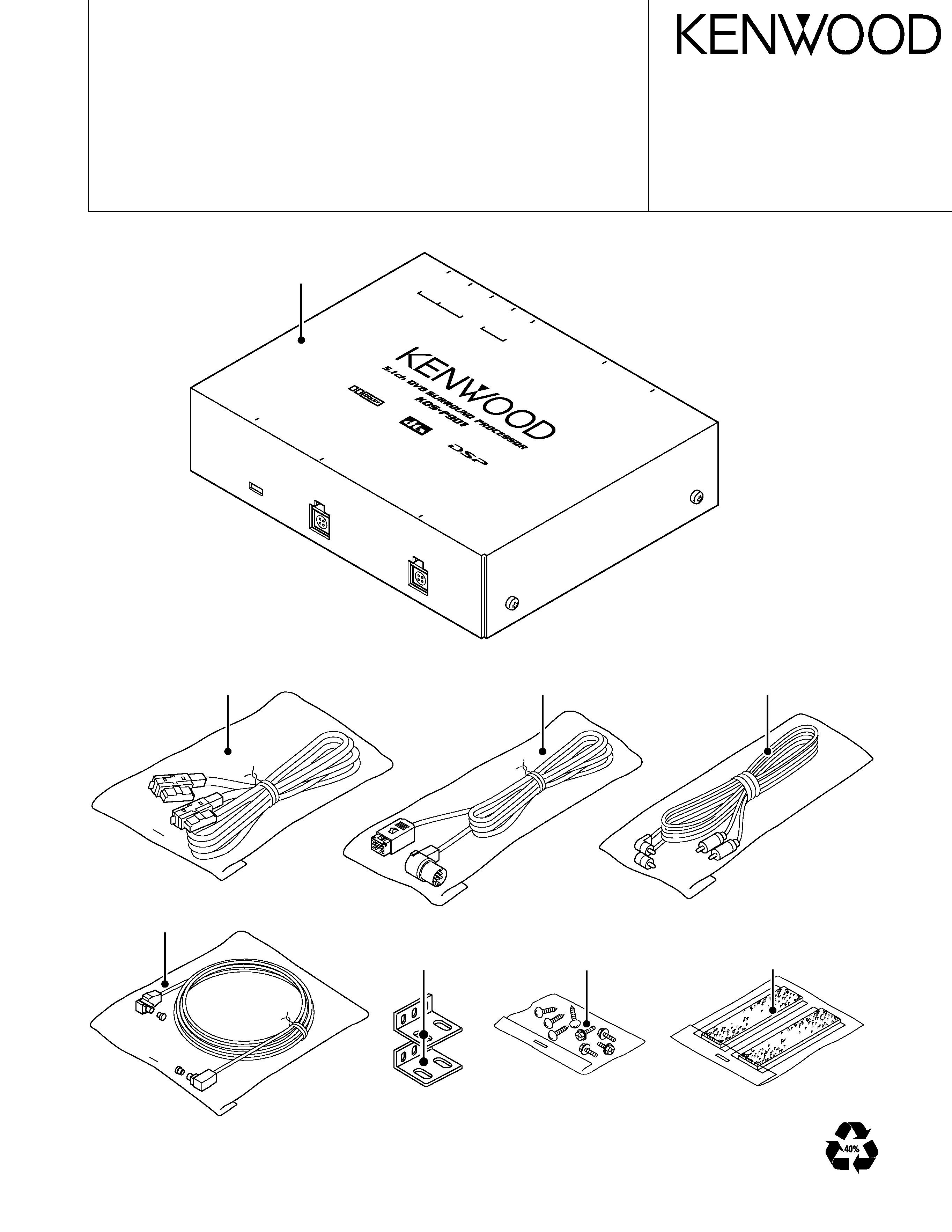
Metallic cabinet
(A01-2743-01)
Mounting hardware
(J21-3801-04)x2
Cord with plug
(E30-4740-05)
Cord with pinplug
(E30-6014-05)
Cord with plug
(E30-4996-15)
Screw set
(N99-1558-05)
Majic tape
(H30-0051-05)
Cord with connector
(E30-4938-15)
KDS-P901
2
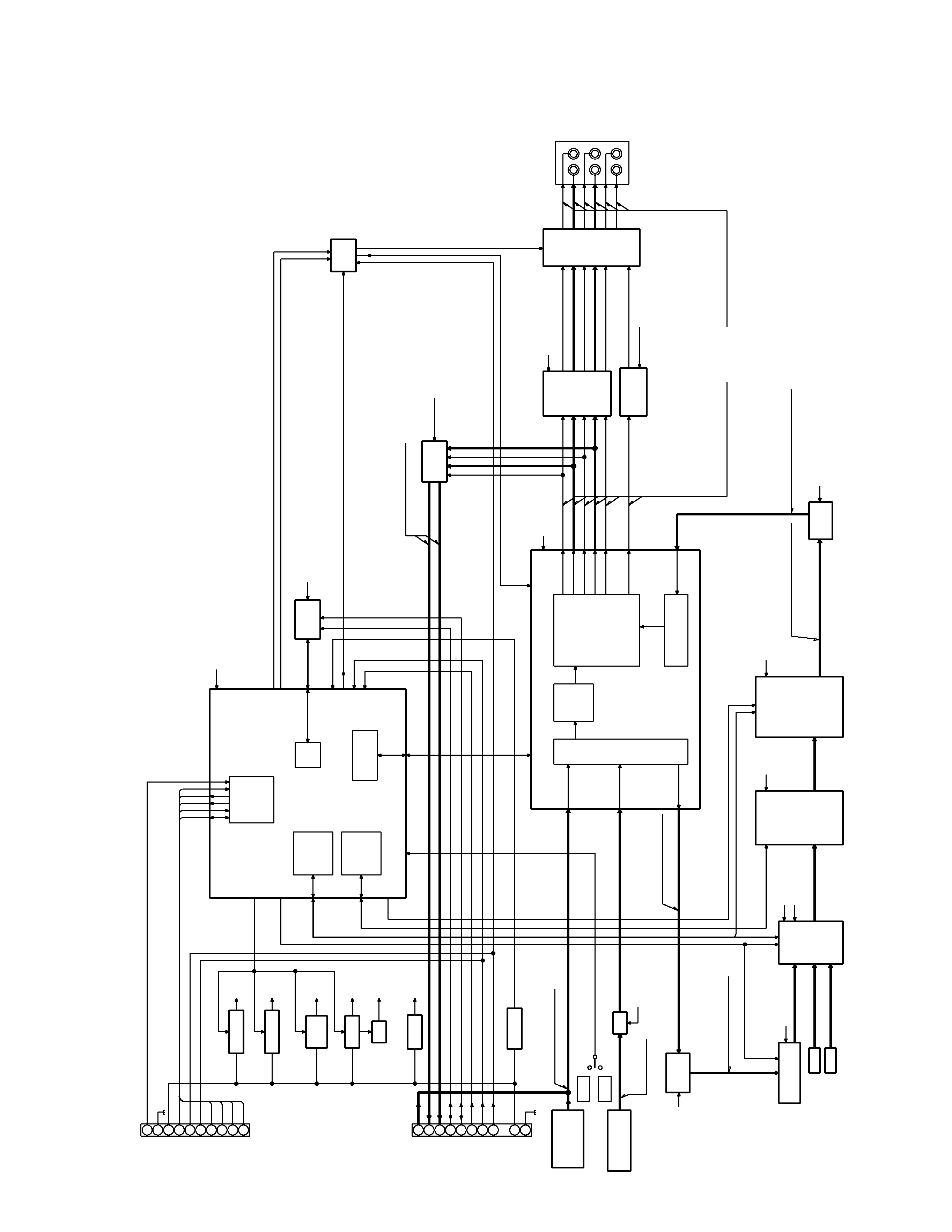
BLOCK
DIAGRAM
A8V AVR
A5V AVR
D3.3V
SW9V
-9V
B.U5V
MZ-BUS
SYSTEM u-COM
B.U DET
MZ-BUS CN
SEL
TDA7501
EVOL
+6dB
INPUT GAIN
ISO
(BUS)/
(+4.6dB)
BUFFER
CONVERTER
A/D
DIR
D IN
D IN
DSP
6ch D/A
CONVERTER
L.P.F
(-6.5dB)
(CD IN)
+3dB
2ZONE
VOL
ANALOG : +2dB
DIGITAL : 0dB
2ZONE : 0dB
BUFF
(-3dB)
MUTE
PRE AMP
(9.1dB)
(9.1+15dB)
PRE AMP
PRE OUT
(5L)
(FOR DVD/R)
5L IN
AV/AUX IN
(5L)
5L
BUS
(BUS)
MUTE
CONT
5L-CONT CN
(5L)
AVR
Q13,14,17
Q11,12
IC15
IC14
IC9,Q16
Q1-3,7-10
Q4-6
IC10
Q18,19
IC1
IC13
DRIVER
IC28,29
Q106,107,
IC26,31,32
499-501
IC5
Q104
S1
IC8
IC30
IC4
IC3
IC2,16-18
IC6
IC20-22
IC23(1/2),24,25
Q502-507
IC23(2/2)
A8V
A5V
D3.3V
SW9V
SW-9V
B.U5V
PON
SYS ON
RESET
MUTE
CDTI
CCLK
CDT0
ERF
CS
DIR
DSP
SS
CLK
DRST
SI
S0
IERX
IETX
IEON
BUDET
B.U5V
DAPD
CLK
DATA
SEL
EVOL
B.U5V
BUS+
B.U
GND
MUTE
BUS ON
RESET
BUS-
REAR OUT
FRONT OUT
AUDIO I/O
CD IN
A8V
A5V
A3.3V
D3.3V
D3.3V
A5V
A8V
CASS IN
A OUT
RR
RL
FR
FL
CENTER
SUB
FRONT L,R
REAR L,R
SW9V,-9V
CENTER
SUB
FR
FL
RR
RL
SW9V,-9V
SW9V
A8V
SW9V,-9V
DIR RST
ERF
D
ATA
C
REQ-H
CHCON
5L
CLK
D
ATA
H
REQ-C
BUS/5L-SW
BUS/5L-SW
S MUTE
MUTE F
MUTE R
DATAH
CLK
REQ-H
GND
B.U
RST
CHCON
REQ-C
DATAC
MUTE
200mV
600mV
1200mV
ANALOG
AV
AV
FM,TV
CD,MD,DVD,CH
ANALOG
AM
720mV
240mV
1400mV
240mV
1840mV
1400mV
120mV
680mV
CD,DVD,CH
340mV
110mV
DIGITAL
680mV
ANALOG
750mV
4500mV
4500mV
2250mV
4500mV
4500mV
285mV
1700mV
1700mV
850mV
300mV
1700mV
480mV
240mV
ANALOG
80mV
480mV
200mV
1200mV
1200mV
600mV
1200mV
:
:
:
: 800mV
400mV
800mV
135mV
FM,TV
AV
AM
:
:
CD,MD,DVD,CH :
:
FM,TV
AV
AM
:
:
CD,MD,DVD,CH :
:
CD,MD,DVD,CH,SUB :
: 865mV
CD,MD,DVD,CH
AM
FM,TV
:
:
:
CD,MD,DVD,CH,SUB
CD,MD,DVD,CH
CD,MD,DVD,CH
DIGITAL
ANALOG
:
AM
AV
:
:
FM,TV
:
:
:
CD,MD,DVD,CH,SUB
CD,MD,DVD,CH
CD,DVD,CH
DIGITAL
ANALOG
:
AM
AV
:
:
FM,TV
:
:
:
CD,MD,DVD,CH,SUB
CD,MD,DVD,CH
CD,MD,DVD,CH
DIGITAL
ANALOG
:
AM
AV
:
:
FM,TV
:
:
:
CD,MD,DVD,CH
CD,MD,DVD,CH
ANALOG
DIGITAL
:
AM
AV
:
:
FM,TV :
:
: 920mV
1200mV
AUX :
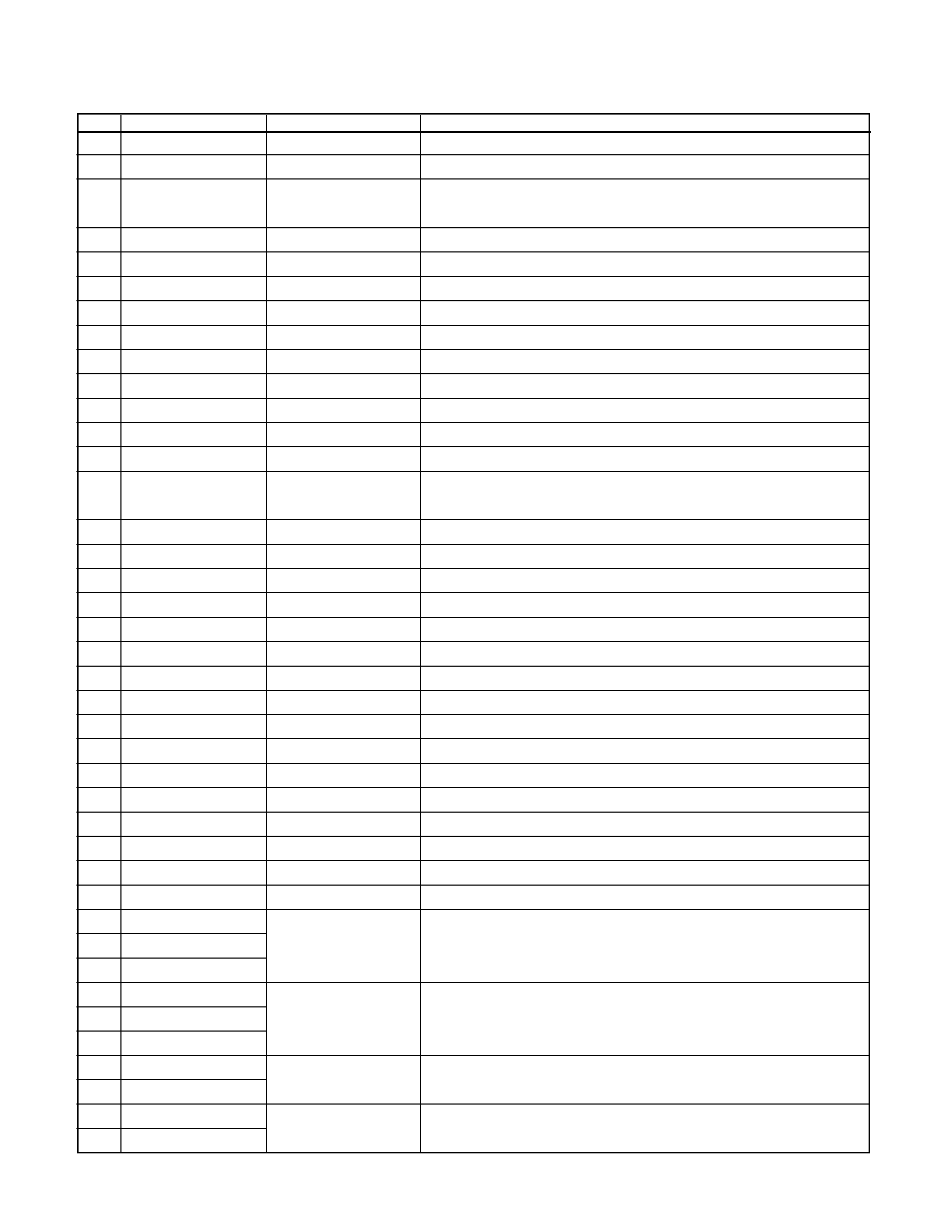
IC1
703037AGF-A05
System MI-COM.
IC2
DSP56362PV100
DSP IC
IC3
AK4112A
DIR
Digital audio receiver
(for AES/EBU, IEC958, S/P DIF, EIAJ CP1201)
IC4
AK5353VT
A/D converter
IC5
TDA7501
E-VOL.
IC6
AK4356VQ
D/A converter
IC7
TC7WU04FU
Inverter
Resonator for DSP IC
IC8
BA3121F
Isolation IC
AUX IN isolation amplifier
IC9
LM2595S-ADJ
Switching regulator
D 3.3V AVR
IC10 MC33063AD
Switching regulator
-9V AVR for PRE OUT amplifier
IC12 S-80842ANNP
Reset IC
When BU 5V voltage is less than 4.2V, IC outputs Lo.
IC13 HA12187FP
BUS IC
BUS communication IC
IC14 BA178M05T
AVR IC
IC outputs 5.0V for A 5V lines.
IC15 M5237ML
AVR IC
IC is combined with Q11, and it works as the error
detection, the driver.
IC16 AS7C31026-12JC
SRAM
1M(65,536 words X 16bits)
IC17 AS7C31026-12JC
SRAM
1M(65,536 words X 16bits)
IC18 MR27V401D-16TA
ROM
dts ROM
IC19 NJM4565M-TE2
OP AMP
Reference voltage output buffer (+4V output)
IC20 NJM4565M-TE2
OP AMP
D/A converter output LPF(for CENTER and SUB channels)
IC21 NJM4565M-TE2
OP AMP
D/A converter output LPF(for FL and FR channels)
IC22 NJM4565M-TE2
OP AMP
D/A converter output LPF(for RL and RR channels)
IC23 NJM4565M-TE2
OP AMP
PRE OUT amplifier(for CENTER and SUB channels)
IC24 NJM4565M-TE2
OP AMP
PRE OUT amplifier(for FL and FR channels)
IC25 NJM4565M-TE2
OP AMP
PRE OUT amplifier(for RL and RR channels)
IC26 TC7W02F
2-inputs NOR x2
Mute logic(BRST+MUTE, BUDET)
IC28 NJM4565M-TE2
OP AMP
BUS audio output buffer(for FR and RR channels)
IC29 NJM4565M-TE2
OP AMP
BUS audio output buffer(for FL and RL channels)
IC30 NJM4565M-TE2
OP AMP
A/D converter input buffer
IC31 TC7W02F
2-inputs NOR x2
Mute logic(MUTEF+BMU, MUTER+BMU)
IC32 TC7S08F
2-inputs AND
Mute logic(FMU AND RMU)
Q1
2SC4081
Q1and Q3 work as a differential amplifier, Q2 works as a driver,
Q2
2SA1037K
PRE-AMP +9V AVR
and +9V is supplied to OP AMP.
Q3
2SC4081
Q4
2SA1037K
Q4and Q6 work as a differential amplifier, Q5 works as a driver, and
Q5
2SC4081
PRE-AMP -9V AVR
-9V is supplied to OP AMP.
Q6
2SA1037K
Q7
2SC4081
A9V AVR
When Q7's base becomes Hi, AVR outputs +9V.
Q8
2SB1184
Q9
DTA124EUA
A9V AVR SW
When Q10's base becomes Hi, AVR SW is turned on.
Q10
DTC124EUA
KDS-P901
3
COMPONENT DESCRIPTION
q PROCESSOR UNIT(X32-4990-01)
Ref.No.
Component Name
Application / Function
Operation / Condition / Compatibility
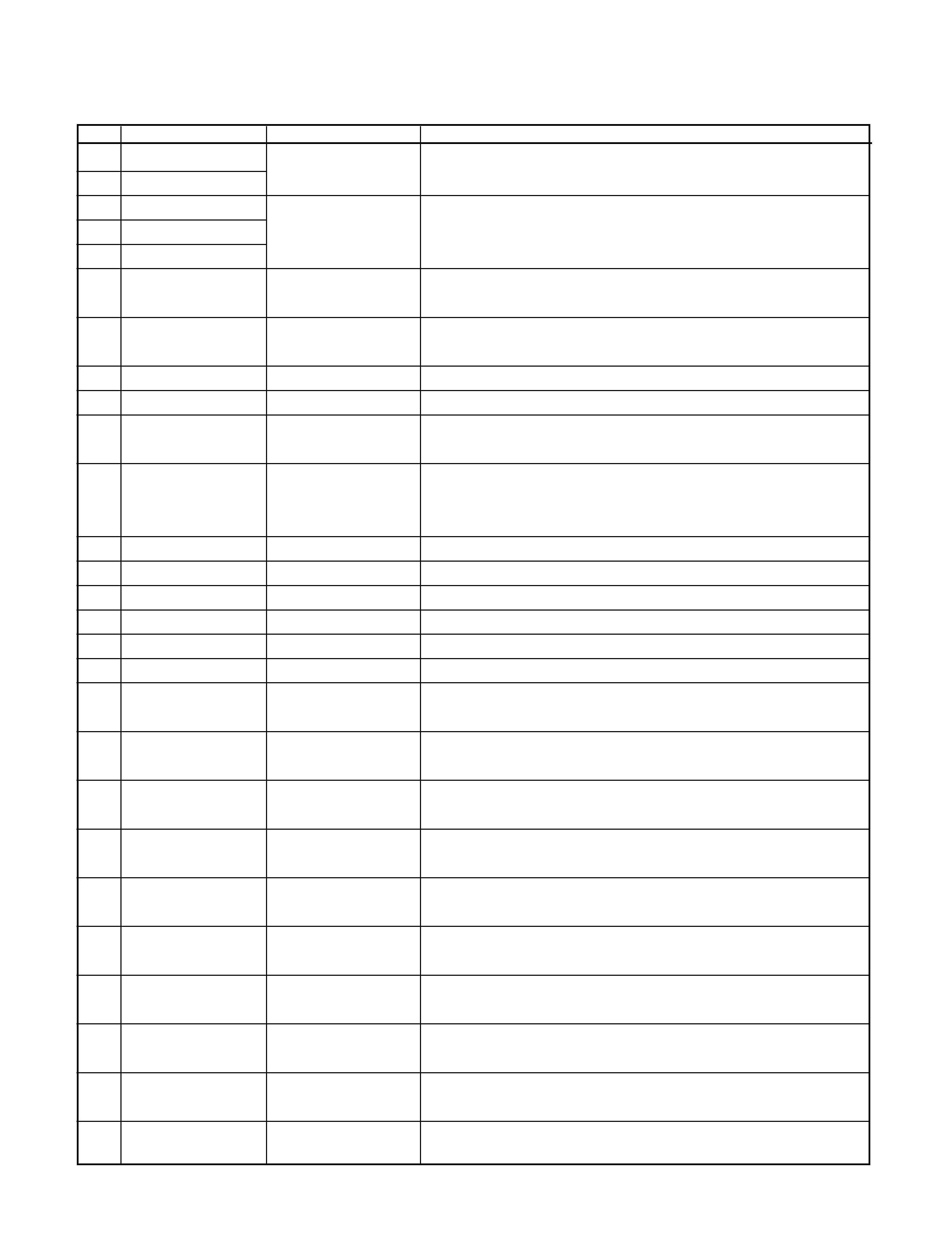
Q11
2SB1565(E,F)
A 8V AVR
When Q12's 2 pin becomes Hi, AVR outputs +8V.
Q12
UMC2N
Q13
2SC4081
Q14
2SB1565(E,F)
A 5V SW
When Q17's 2 pin becomes Hi, AVR SW is turned on.
Q17
UMC2N
Q16
DTC144EUA
D 3.3V SW
When a base becomes Hi, Q16 is turned on, and D
3.3V AVR outputs +3.3V.
Q18
2SC4081
BU 5V AVR
While BACKUP is applied, Q18's base becomes Hi,
Q19
2SB1565(E,F)
and AVR outputs +5V.
Q101 DTB123YK
PON5V SW
When a base becomes Lo, Q101 is turned on.
Q102 DTC144EUA
CH CON SW
While Q102's base becomes Hi, the control from H/U side is working.
Q103 DTC144EUA
System ON/OFF request SW
When a base becomes Hi, Q103 is turned on, and System ON
request from H/U side is working.
While BACKUP is applied, a base goes Hi, and Q104 is turned on.
Q104 2SC4081
BU detection SW
When momentary power down has detected, a base goes Lo, and
Q104 is turned off.
Q105 DTC144EUA
RESET SW
When a base becomes Hi, System reset is working.
Q106 DTA124EUA
IC26 mute SW
When a base becomes Lo, Audio mute is working.
Q107 DTC144EUA
BUS MUTE invert SW
When BUSMUTE(BMU) becomes Hi, Q107 is turned on.
Q201 2SK3018
Level shifting
FET for the level shifting between 3.3V and 5V
Q202 2SK3018
Level shifting
FET for the level shifting between 3.3V and 5V
Q204 2SK3018
Level shifting
FET for the level shifting between 3.3V and 5V
Q301 DTC143TUA
E-VOL. mute SW
When a base becomes Hi, Q301 is turned on, and E-V0L. mute
is working.
Q499 UMC5N
PRE-OUT mute driver
When Q499's 2 pin becomes Hi, Q499 is turned on, and Mute is
working in CENTER/SUB outputs.
Q500 UMC5N
PRE-OUT mute driver
When Q500's 2 pin becomes Hi, Q500 is turned on, and Mute is
working in FL/FR outputs.
Q501 UMC5N
PRE-OUT mute driver
When Q501's 2 pin becomes Hi, Q501 is turned on, and Mute is
working in RL/RR outputs.
Q502 2SD2114K
PRE-OUT mute SW
When a base becomes Hi, Q502 is turned on, and Mute is working
in CENTER output.
Q503 2SD2114K
PRE-OUT mute SW
When a base becomes Hi, Q503 is turned on, and Mute is working
in SUB output.
Q504 2SD2114K
PRE-OUT mute SW
When a base becomes Hi, Q504 is turned on, and Mute is working
in FR output.
Q505 2SD2114K
PRE-OUT mute SW
When a base becomes Hi, Q505 is turned on, and Mute is working
in FL output.
Q506 2SD2114K
PRE-OUT mute SW
When a base becomes Hi, Q506 is turned on, and Mute is working
in RR output.
Q507 2SD2114K
PRE-OUT mute SW
When a base becomes Hi, Q507 is turned on, and Mute is working
in RL output.
KDS-P901
4
COMPONENTS DESCRIPTION
Ref.No.
Component Name
Application / Function
Operation / Condition / Compatibility
1
DATAC
O
Communication data output to H/U
2
HCLK
I
Communication clock input from H/U
3
MUTE R
O
Rear mute control output
Lo: Mute ON(Rear speaker during
2-zone mode ON, or 2-zone modeOFF)
4
MUTE F
O
Front mute control output
Lo: Mute ON(Front speaker during
2-zone mode ON, or 2-zone modeOFF)
5
DIR CS
O
DIR chip select
Lo: DIR communication permitted
6
DIR CDTI
I
DIR data input
7
DIR CDTO
O
DIR data output
8
DIR CCLK
O
DIR communication clock output
9
EVDD
-
Positive power supply connection terminal
Connected to BU 5V lines.
10
EVSS
-
Ground connection terminal
Connected to GND lines.
11-14
NC
O
Not used(N.C.)
15
DSP SI
I
Data input from DSP IC
16
DSP SO
O
Data output to DSP IC
17
DSP CLK
O
Communication clock output to DSP IC
18
DSP SS
O
DSP communication permission output
Lo: Communication start permitted
19
DIR RST
O
Reset output to DIR IC
Lo: Reset
20
DSP RST
O
Reset output to DSP IC
Lo: Reset
21
IC/Vpp
-
Internal connection terminal
Connected to GND lines.
22
DA PD
O
D/A converter power down SW
Lo: Power down, internal register clear
23
P ON
O
P ON control output
Hi: OFF, Lo: ON
24,25
NC
O
Not used(N.C.)
26
IERX
I
IE bus input
27
IETX
O
IE bus output
28,29
NC
O
Not used(N.C.)
30
IE ON
O
IE bus IC control output
Hi: Bus communication permitted,
Lo: Standby
31
BUS/5L SW
I
Bus/5L selection SW input
Hi: Bus unit, Lo: 5L unit
32
MUTE
O
MUTE control output
Lo: Mute control OFF,
Hi: Mute control ON
33
NC
O
Not used(N.C.)
34
RESET
I
System reset input
Lo: Reset, Lo . Hi: Operation start
35
XT1
I
Sub clock resonator connection terminal
Not used(pull down to GND lines)
36
XT2
-
Sub clock resonator connection terminal
Not used(N.C.)
37
REGC
I
Regulator oscillator connection terminal
1uF capacitor connected
38
X2
-
Main clock resonator connection terminal
12.58MHz
39
X1
I
Main clock resonator connection terminal
40
VSS
-
Ground connection terminal
Connected to GND lines.
41
VDD
-
Positive power supply connection terminal
Connected to BU 5V lines.
qIC1 (PROCESSOR UNIT: X32-4980-01)
Pin No.
Pin Name
I/O
Description
Processing Operation
5
KDS-P901
MICROCOMPUTER'S TERMINAL DESCRIPTION
