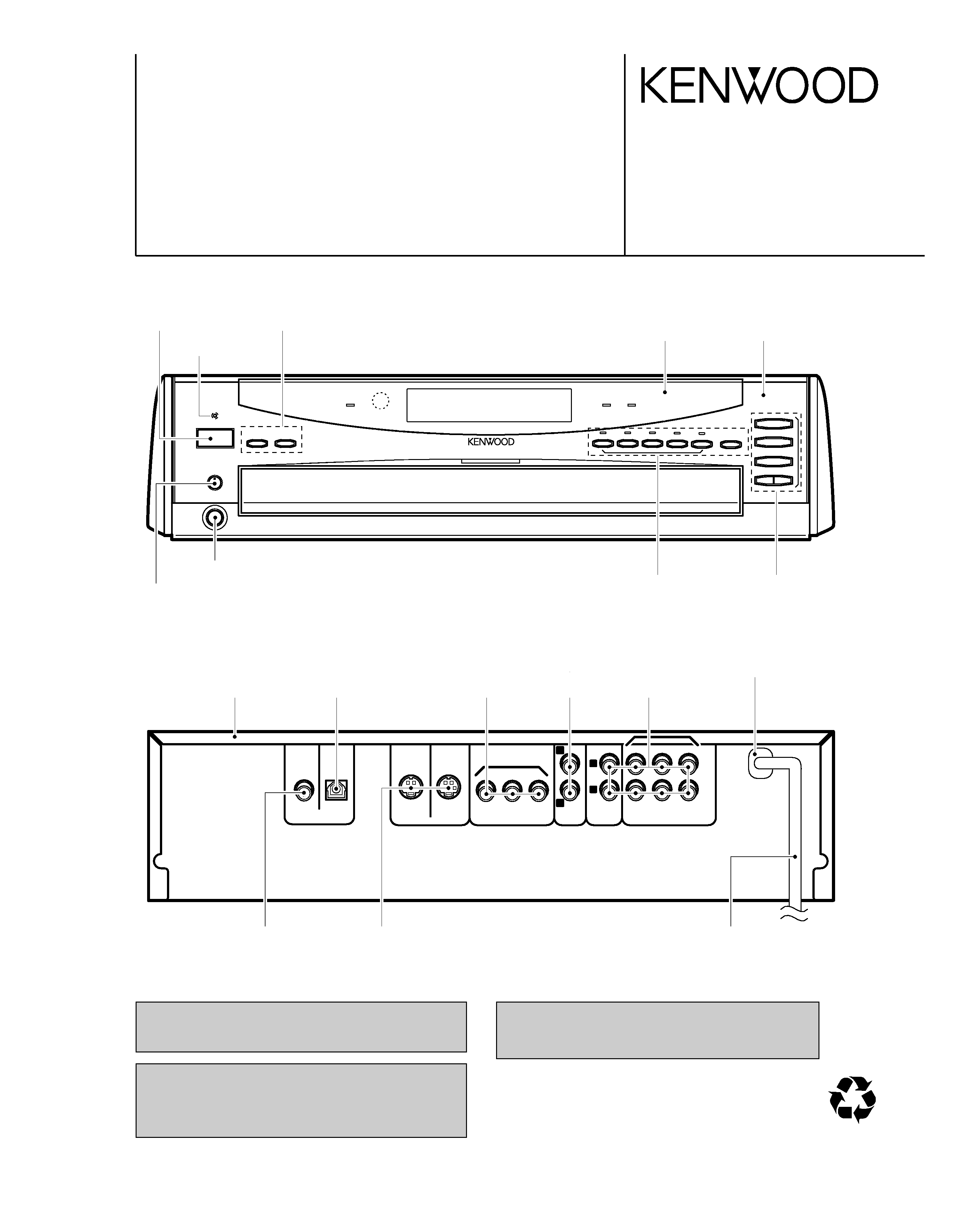
In compliance with Federal Regulations, following are repro-
duction of labels on, or inside the porduct relating to laser prod-
uct safety.
KENWOOD-Crop. certifies this equipment conforms to DHHS
Regulations No.21 CFR 1040. 10, Chapter 1, subchapter J.
DANGER : Laser radiation when open and interlock defeated.
AVOID DIRECT EXPOSURE TO BEAM.
Caution : No connection of ground line if disassemble
the unit. Please connect the ground line on
rear panel, PCBs, Chassis and some others.
DVD VCD CD PLAYER
© 2000-9/B51-5665-00 (K/K) 3473
STANDBY
POWER
DISC SKIP
PHONES LEVEL
PHONES
MIN
MAX
- ON OFF
DISC
1
PURE AUDIO
MODE
DISC
2
DISC
3
DISC
4
DISC
5
OPEN/CLOSE
0
3
8
7
¢
4
SAMPLING
96kfs
192kfs
VIRTUAL
SURROUND
0 0
00
0
00000000000
ANGLE
RAMDOM
PGM
P.B.C.
P.PCM
MPEG
DOLBY
DTS
REPEAT TEXT
INDEX
INDEX
SEQ.1
SEQ.2
D.MIX
TOTA L
VIDEO
AUDIO
DIGITAL
DVD
CD
VCD
1
1
2
3
3
4
4
5
5
2
A
A
B
3
DVD
COAXIAL
OPTICAL
DIGITAL OUTPUT
(PCM/BIT STREAM)
SUB WOOFER
FRONT SURROUND
6CH. OUTPUT
COMPONENT VIDEO OUTPUT
YCb
Cr
1
2
MIX LINE
OUTPUT
VIDEO
OUTPUT
L
R
CENTER
S1 VIDEO
OUTPUT
S1/S2 VIDEO
OUTPUT
Knob
(K29-7805-13)
Phone jack
(E11-0190-05)
Indicator
(B12-0399-14)
Metallic cabinet
(A01-3759-01)
Pin jack
(E63-1158-05)
Pin jack
(E63-1128-05)
Oscillating module
(W02-2732-05)
Front glass
(B10-3608-02)
Panel
(A60-1846-12)
Pin jack
(E63-1156-05)
AC power cord bushing
(J42-0083-05)
AC power cord
(E30-2909-05)
Pin jack
(E63-1171-05)
Cylindrical receptacle
(E56-0031-05)x2
Knob
(K29-7806-13)
Knob
(K29-7194-04)
DV-4070-B/4900
SERVICE MANUAL
DVF-R7030-B/R9030
Knob
(K27-2408-14)
Knob
(K29-7803-04)
70%
Illust. is DV-4900.
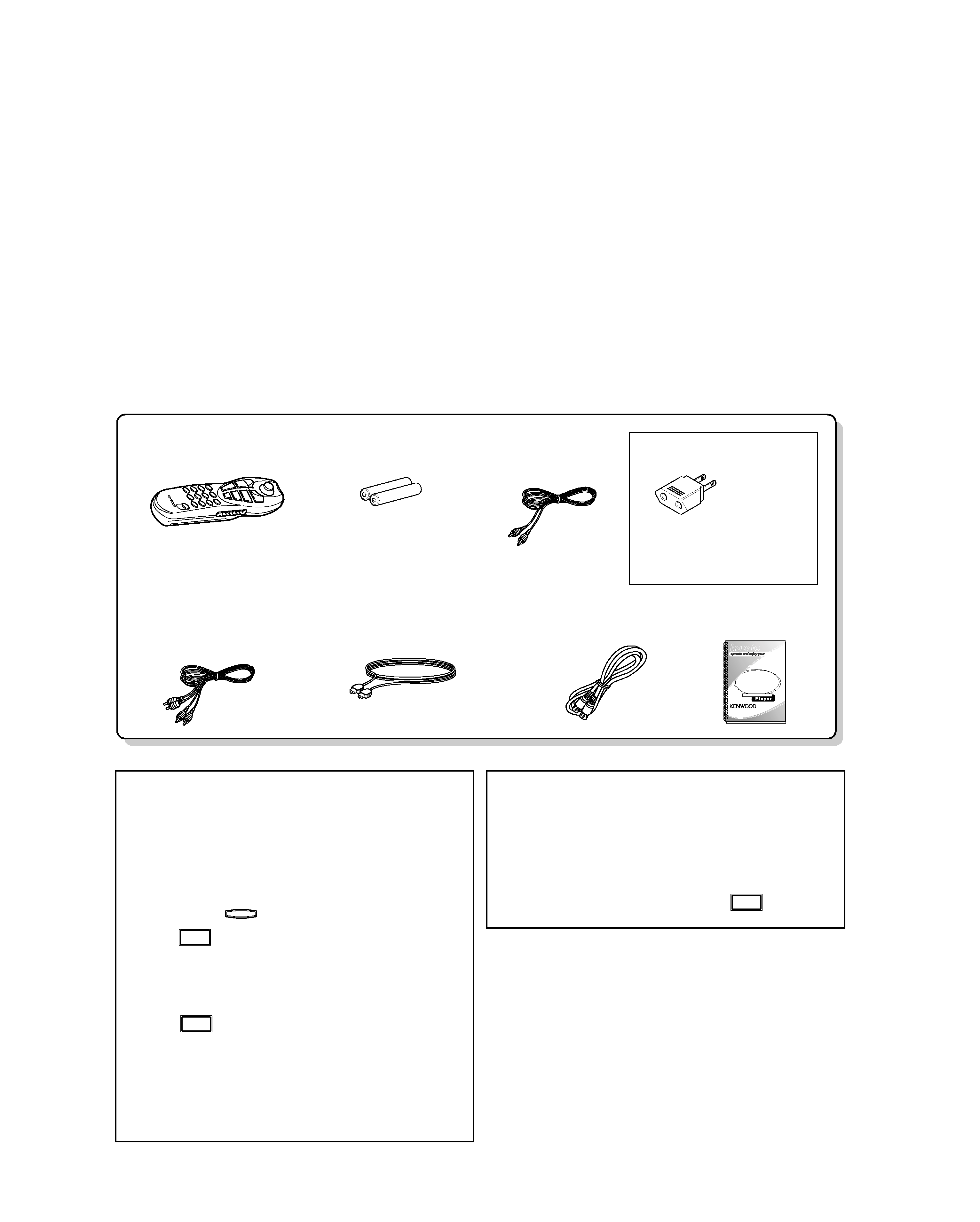
Multiple D VD VCD CD
Instructoin manual/
separate User's Guide (1)
Joystick remote control unit (1)
(A70-1412-05)
Battery cover(A09-1124-08)
Batteries (R6/AA)(2)
Video cable(1)
(E30-1427-05)
AC plug adapter (1)
(E03-0115-05)
Use to adapt the plug on the
power cord to the shape of the
wall outlet.
(Accessory only for regions
where use is necessary.)
S Video cable(1)
(E30-2956-05)
Audio cables(3)
(E30-0505-05)
Optical fiber cable(1)
(B19-1529-05)
DV-4070-B/4900/DVF-R7030-B/R9030
2
CONTENTS / ACCESSORIES
CONTENTS / ACCESSORIES .................................. 2
DISASSEMBLY FOR REPAIR....................................3
CIRCUIT DESCRIPTION ............................................5
ADJUSTMENT ..........................................................17
PARTS DESCRIPTIONS ..........................................18
PC BOARD ...............................................................19
SCHEMATIC DIAGRAM .......................................... 23
EXPLODED VIEW ....................................................41
PARTS LIST..............................................................43
SPECIFICATIONS ....................................................54
Contents
Accessories
Malfunction of Microcomputer
In case the microcomputer malfunctions, making operations
impossible or showing wrong messages on the display even
if you connected everything properly. When the microcom-
puter malfunctions, perform the following procedure to reset
the microcomputer and return it to the normal condition.
1. While holding
on the player main unit,
press
.
2. The display on the main unit shows blinking "INIT" (ini-
tializing), then shows "INIT OK!" (Initialization OK) to
indicate that the microcomputer is reset.
3. Press
on the main unit to turn it off, then press
it again to turn it on.
¶ The resetting clears the setups stored in the microcom-
puter and returns it to the factory-set initial condition.
After resetting, you should perform the various setups
of the player again from the beginning.
POWER
- ON OFF
POWER
- ON OFF
7
Transport or moving precautions
When transporting or moving the player, first remove the
disc and observe the following procedure.
1. Turn the player power on.
2. Wait for a few seconds, until the display shows "NO
DISC".
3. Turn the player power off by pressing
.
POWER
- ON OFF
Note: Please contact our KENWOOD Service Department in your side if you want the information;
Main Microprocessor(MN10102LP25G),Sub Microprocessor(MN101C28C) ports explanation,
D.R. I.V.E. ¿ and SCART Circuit Description and full(previous) format Parts list on this
model. You can be available them by internet from us.
DV-4070-B/4900/DVF-R7030-B/R9030
3
DISASSEMBLY FOR REPAIR
1
5
2
3
6
4
5
HOOK (
x2)
HOOK
x2
Guide
6
3
4
HOOK
GUIDE
ARM
DRIVE
GEAR
HOOK
LOADING
GEAR (A)
(Free)
PROTRUSION OF TRAY
2
1
5
REAR
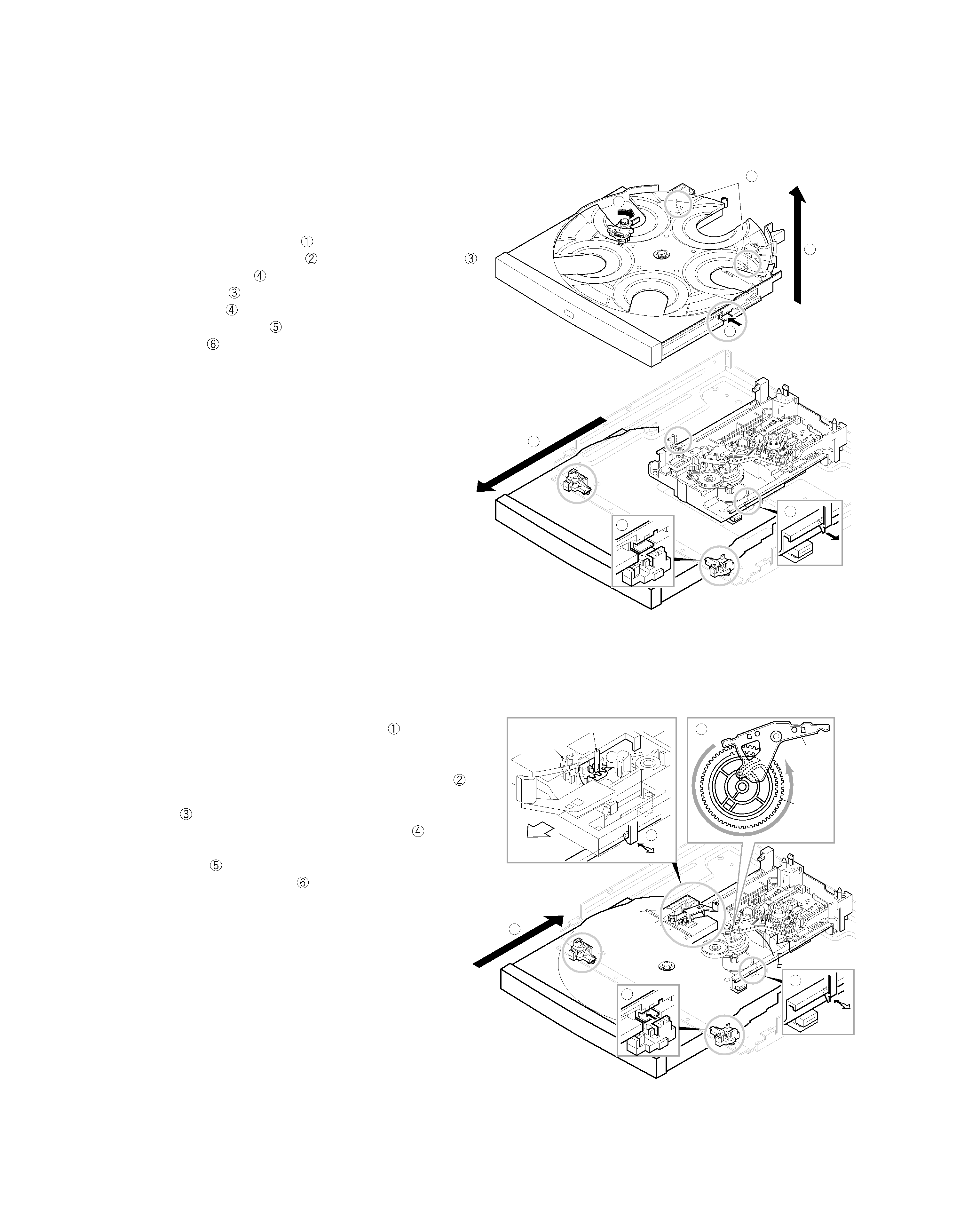
1. How to Remove Tray
1. Remove the front panel and flexible cable.
Disassemble the X25 and power supply pcb with sub
chassis if it is a difficult.
2. Push and hold the lever(
)to clockwise and pull barely
out the tray to frontwards(
) where the hook of tray(
)
meets with guide(
).
3. Push hooks(
), both sides, inwards and release them
from guides(
).
4. Pull hooks of tray(
) outwards and remove the tray
upwards(
).
2. How to Assemble Tray
1. Adjust the position of drive gear as figure(
).
Check traverse unit is at the lowest position.
2. Load the tray on the loading mechanism.
Check the position where the loading gear(A) is free(
)
3. Meet the hooks with guides and push hooks to load the
tray(
).
4. Set the right side hook to loading mechanism(
).
5. Set the left side hook to loading mechanism with pulling it
outwards(
).
6. Push the tray backwards(
).
DV-4070-B/4900/DVF-R7030-B/R9030
4
DISASSEMBLY FOR REPAIR
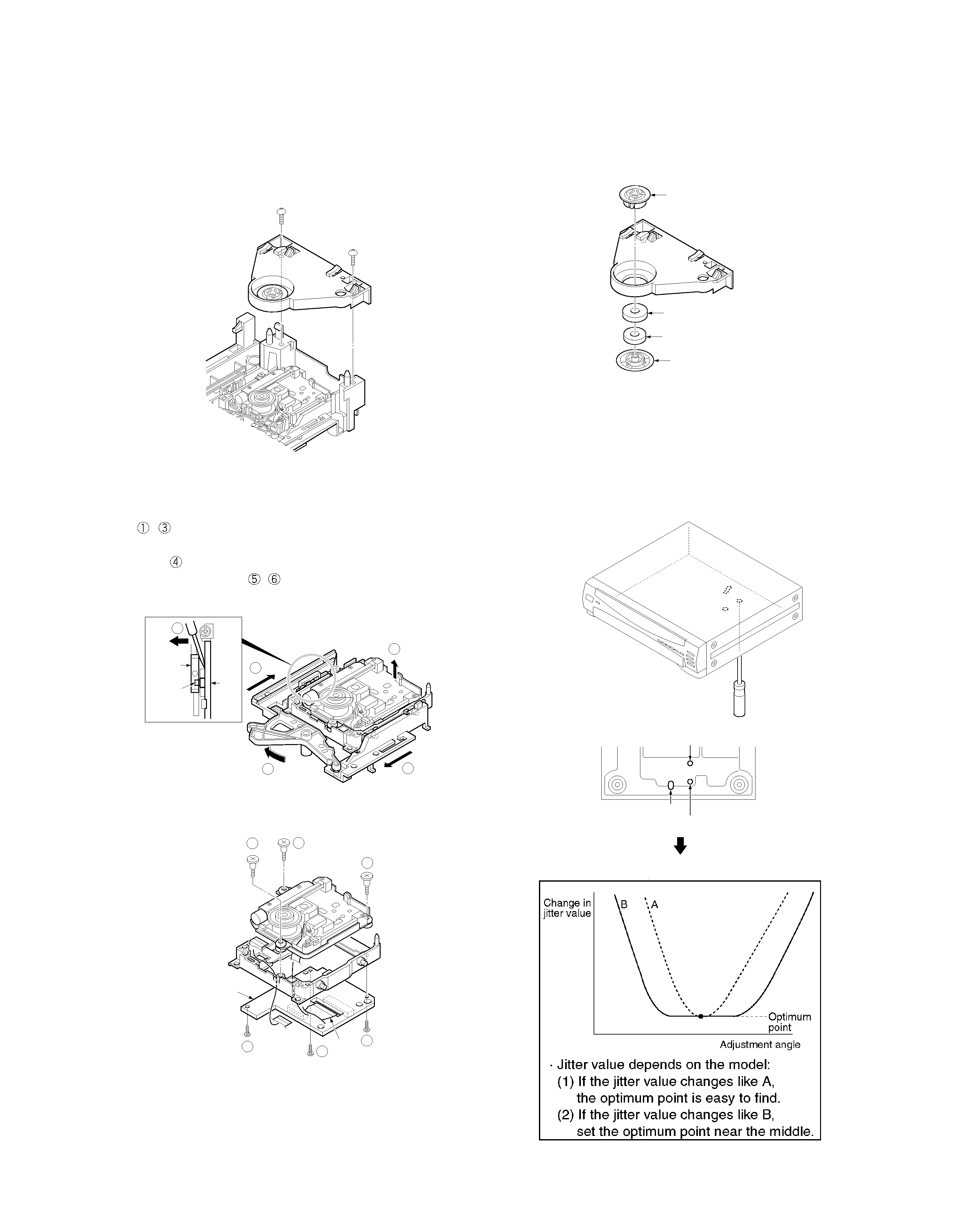
5. How to Disassemble Traverse Unit
1. Move the traverse to upward by turning motor pulley
(
~
).
2. Make the gap between the tray guide and guider(L) with
driver(
)
3. Remove the screws(
,
).
2
4
2
1
3
Tray
guide
Guider
(L)
Protruding
part
5
5
5
6
6
6
X13-7770-10
CN1
CN2
Clamper weight
Spacer
Magnet
Clamper
3. How to Remove Clamper Ass'y
1. Remove screws.
4. How to Disassemble Clamper Ass'y
6. Tangential and Tilt Adjustment
1. Turn the power on with pressing the DISC 1 key.
(Display shows "INSPECTION"; test mode.)
2. Press the DISC1 key in playback mode again.
Display shows "Jitter *** %"
3. Turn off if cancel test mode.
REAR
Tilt adjustment screw 2
Tilt adjustment screw 1
Tangential adjustment screw
DV-4070-B/4900/DVF-R7030-B/R9030
5
CIRCUIT DESCRIPTION
Port No.
Port Name
I/O
Description
1
WAIT
O
Optical Device Control(ODR) wait
2
NRD
O
Read(RD) port for ODC/AV
3
-
-
No use
4
NWA
O
write(WR)
5
RAMCS
O
Chip Select(CS) Flash RAM
6
ODCCS
O
Chip Select(CS) ODC
7
AVCS
O
Chip Select(CS) AV decoder
8
RAMCS
O
Chip Select(CS) DRAM for TEXT buffer
9
SCLOCK
O
Clock of Video DAC(ADV7172)
10
SDATA
O
Data of Video DAC(ADV7173)
11
FRD
O
Read(RD) port for Flash ROM
12
MODE2
I
H: Chip Select 0, 8bit bus
13-16
CPUADR0-3
O
Address A(0-3)
17
Vdd
I
+5V
18
SYSCLK
O
AV decoder HCLK
19
Vss
O
GND
20
XI
I
Clock input port
21
XO
O
Clock output port
22
Vdd
I
+5V
23
CLK
I
13.5MHz clock input port
24
OSCO
O
No use
25
MODE2
I
CPU mode: H=Memory enhanced mode
26-33
CPUADR4-11
O
Address A(4-11)
34
Vdd
I
+5V
35-42
CPUADR12-19
O
Address A(12-19)
43
Vss
-
GND
44
196BSY
I
Busy of writing jig
45
256BSY
O
Busy of unit
46
ATTL
O
Analog output attenuator L: active
47
-
-
No use
48
KMODE
I
writing mode. H=writing. L=normal.
49
AMUTE
O
Audio mute
50
ADSCEN
I
CIRC enable
51
-
O
No use
52
SLEEP
O
Front End Processor(AN8825) standby
53
FRNTH
O
Front DAC selector. H=front.
54
Vdd
-
+5V
55
FEPEN
I
Front End Processor SEN
56
CLKSEL
O
Sampling frequency selector. L=44,88,176kHz, H=48,96,192kHz
57
STBDAC2
O
DAC2(AK4393) Strob
58
STBSP
O
Serial/parallel(NJU3711) Strob
59
STBDAC1
O
DAC1(AK4393) Strob
60
ADSC
O
Advanced Digital Servo Control serial data transfer.
61
Vss
O
GND
62
-
O
No use
63
XS
O
Chip Select of E2PROM
64
SCSIEN
O
Enable control of writing jig. L=enable
65
DARK-DET
I
Video signal check by Y-signal
66
Vdd
I
+5V
67
SCLKO
O
Sub-microprocessor clock
68
SIO
I
Sub-microprocessor data input
69
SOO
O
Sub-microprocessor data output
70
SCLKI
O
Clock for every Ics
MAIN MICROPROCESSOR: MN102LP25G(X35,IC500)
