DPX-8030MD
2002-4 PRINTED IN JAPAN
B51-7924-00 (4) 517
MD CD DSP RECEIVER
C
V
o
lu
m
e
C
o
n
tr
o
l
COMPACT
DIGITAL AUDIO
TEXT
SCRL
DISP
ANG
SCN
RDM
G.RDM
REP
TUNE/SEEK
M.RDM
PWR OFF
FM+
AM
CRSC
DISC
ATT
DSP
EJECT
CD
EQ
SEL
S.A
Anti-Theft System Installed
NAME
RTN
ANGLE
MD
MD CD DSP RECEIVER
50Wx4 MOS FET
MDLP
FNC
CLK
System E's+
DEMO
SRC
AUD/
over
X
This service manual dose not include information on the CD and MD mechanism assembly (exploded view, parts
list, schematic diagram and mechanism oparation description).
For such information, please refer to the CD mechanism assambly service manual (X92-4470-00 : B51-7899-00)
and MD mechanism assambly service manual (X92-4570-00 : B51-7887-00).
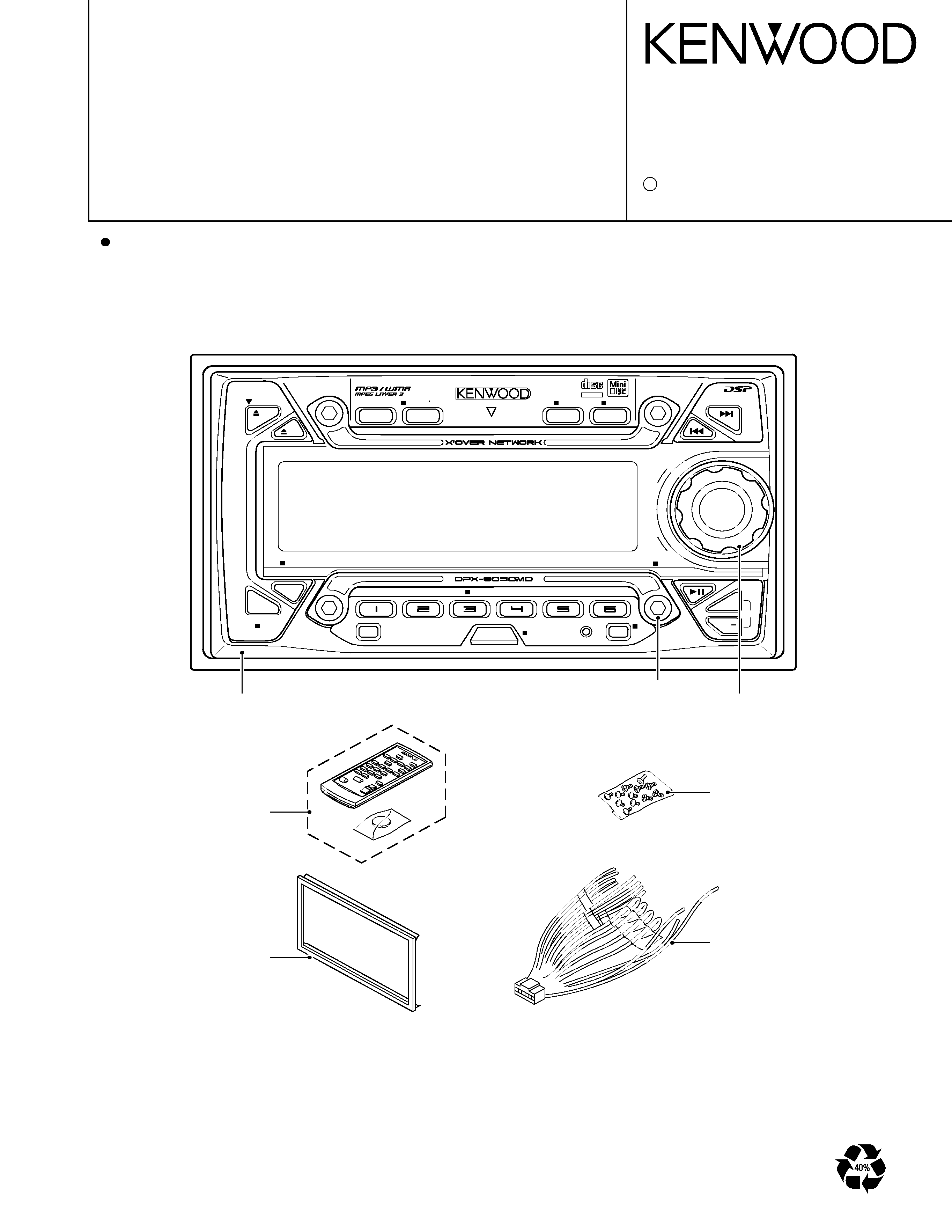
KNOB (VOL.)
(K23-1064-03)
SCREW SET
(N99-1724-05)
PANEL ASSY
(A64-2731-02)
MACHINE SCREW
(N09-6027-05)
REMOTE
CONTROLLER
ASSY
(A70-2028-05)
ESCUTCHEON
(B07-3025-02)
DC CORD
(E30-4939-05)
SERVICE MANUAL

2
D
P
X
-8030
M
D
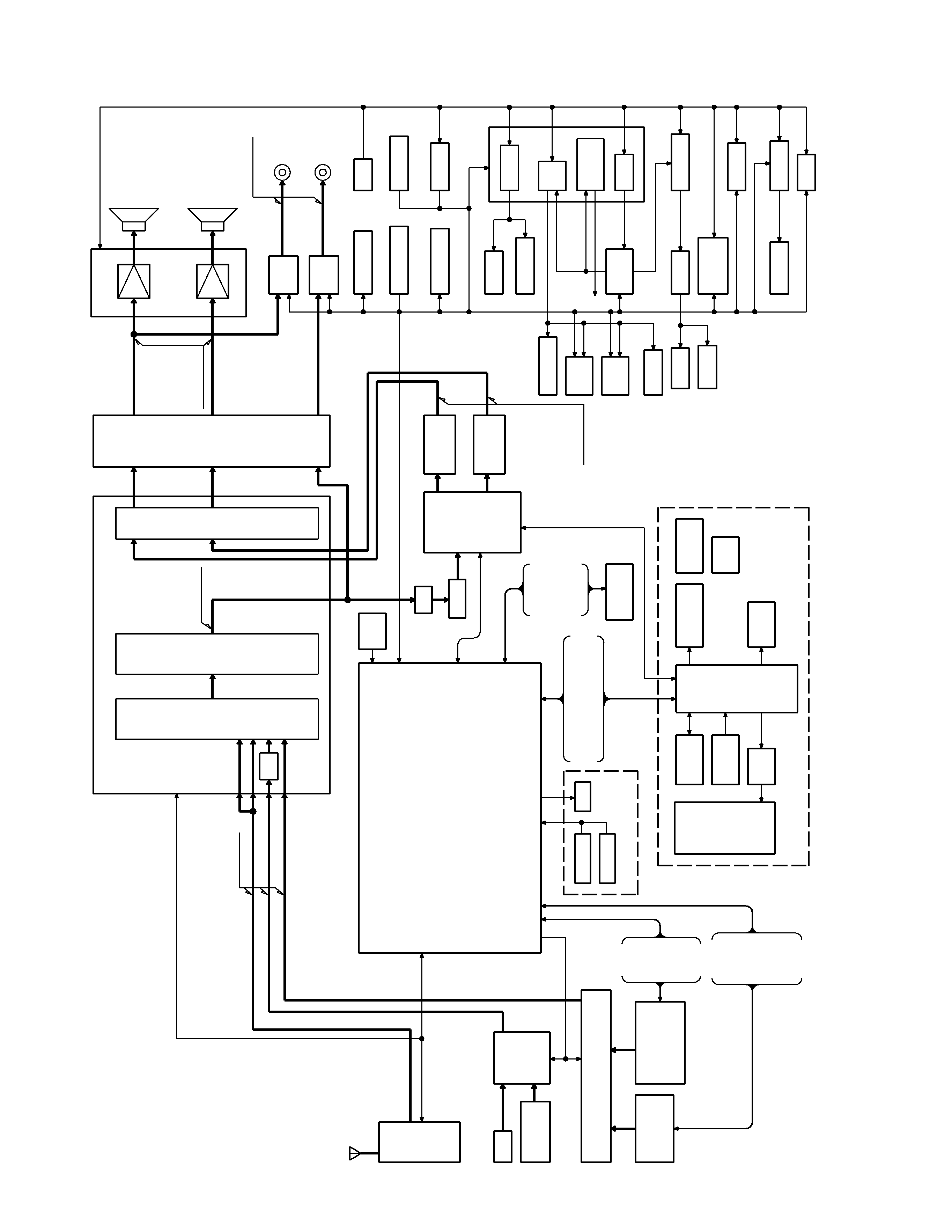
DSP DATAIN
DSP DATAOUT
DSP CLK
DSP SEL
DSP RST
A8V
FM+B
TUN5V
AM+B
CLK
DATA
FM
AM
FSD
FMSD
MD
DET
CD
DET
LED
OPEN
SP REQ
SP DATA
SP CLK SP INT CTS
SC DATA RTS
MC DATA SC CON
FSD
VREF
PMDET
PMOT2
PMOT1
PMODE
OPEN SW
SW1-3
AMUTE
MRST
MSTOP
LO/EJ
MOTOR
DATA M
M CLK
M RST
M STOP
LOE SW
A MUTE
M DATA
M CLK
LOS SW
LOAD
EJECT
CH
TAPE
SYSTEM u-COM
BU5V
VOL
PWR IC
MUTE
F/E
PRE OUT
FRONT
REAR/NF
PRE OUT
DSP
A8V
LPF BUFF
u-COM
LPF BUFF
A8V
DSPA3.3V
ISO
INPUT
SEL
SW
AUX
MD/CD CH
ANALOG
A8V
MD DET
LED
UNIT
A8V
BU5V
RST
M+,M-
P MECHA
BU5V
MATRIX
KEY
FL
X25 UNIT
REMOCON
REMO+B
BU5V
REMO+B
RST SW
3.3V
BUFF
BU5V
B. U.
MUTE
AMP CTRL
SMALL DET
LINE MUTE
BU DET
B. U.
ANT CON
SW14V
A8V
BU5V
DSP3.3V
CD SRV
CD D+B
DC/DC+B
PON5V
DC/DC
MD SRV
DSPA3.3V
FM+B
AM+B
1/2VCC
FL55V
FLFAC
PANEL
5L
DXM-6502W(J)
BU5V,A8V
SRV+B,SW5
E-VOL
MDS-3200W
SRV+B
BU5V,A8V
A8V
ANALOG SW
CD DET
PON5V
X16
FL55V
FL3.3V
ROM
BU3.3V
3.3V
BU5V
MUTE
LPF
SYSTEM
E'S
ACC DET
P CON
PN M DR.
SW16V
E-VOL
MUTE
DSPD3.3V
DXM-6500W(M)
FLFAC
ILL+B
IC2
IC1
IC5
IC12
IC10
IC11
IC3
IC9
IC14
IC4
IC6
IC4
IC3
IC8
IC15
IC7
ATT.
SP OUT
AUX : 1494mV
CH : 3512mV
CD : 3512mV
MD : 3512mV
AUX : 511mV
MD : 1346mV
CD : 1346mV
CH : 1346mV
MD : 786mV
AM : 249mV
CH : 786mV
CD : 786mV
FM : 352mV
AUX : 298mV
CH : 3277mV
AUX : 1394mV
CD : 1200mV
MD : 1200mV
AM : 170mV
AUX : 455mV
FM : 320mV
CH : 1200mV
FM : 603mV
AM : 428mV
AM : 626mV
FM : 1979mV
MD : 3277mV
AM : 584mV
CD : 3277mV
FM : 1846mV
BLOCK
DIAGRAM

3
DPX-8030MD
COMPONENTS DESCRIPTION
IC1
IC2
IC3
IC4
IC5
IC6
IC7
IC8
IC9
IC10
IC11
IC12
IC13
IC14
IC15
IC16
IC17
Q1
Q2
Q3
Q5
Q6
Q7
Q8
Q9
Q10
Q11,12
Q13
Q14
Q15
Q16
Q17
Q18
Q19
Q20
Q21
Q22
Q23
Q24
Q25
Q26
Q52
Q53
Q54
-
Input source switching, SP=OUT/PRE-OUT electronic volume.
Generates BU 5V supply from B.UP,
and AUD 8V supply and DSP(D)3.3V supply and PCON output.
CD and MD input switching.
N/F electronic volume.
CD-CH and AUX input switching.
L,R output low-pass filter.
2-ch analog input, 4-ch analog output. (pos/neg phase PWM output)
LPF L,R channel reference supply.
Front L,R output low-pass filter.
Rear L,R output low-pass filter.
BTL Power amplifier.
WMA supply 5.0V, with variable output and on/off.
-
Output goes low on detecting voltage below 4.2 Volts.
Audio mute & power IC mute control.
DSP 3.3V supply.
Switch turns on when BU voltage surges to approx.
18.2 to 18.9 volts or more, and turns off BU detector switch.
Base goes Hi, when BU voltage is applied and turns on. When an instantaneous
voltage drop is detected and BU turns off or when shutoff, the base goes Lo and
turns off. Base goes Hi, and transistor turns on when Acc voltage is applied.
Base goes Hi, and transistor turns on when vehicle lights turn on.
Turns on when base goes Lo and outputs control signal.
Base goes Hi, and transistor turns on when P CON is output.
-
When base of Q8 goes Hi, Q7 turns on and P ANT output.
Turns on when base goes Hi, and applies voltage to PON 5V line.
Turns on when base goes Hi, and turns on CD servo 7.5 volt supply.
When base of Q13 goes Hi, AVR output turns on.
-
When base of Q15 goes Hi, AVR output turns on.
-
Turns SW16V AVR on and off. Turns on when base goes Hi,
and turns on the SW16V output.
SW16V output turns on when Q18 base goes HI.
-
Turns on when base goes Hi, and turns on the 11 volt LED supply.
Turns on when base of Q21 goes Hi and turns on the 11V output.
-
Turns on when base goes Hi, and turns on FAC11V.
Turns on when base of Q24 goes Hi, and turns on FAC11V output.
-
Turns on when base goes Hi, and turns on the WMA DSP 5 volt supply.
Turns on when base goes Hi, and turns on LED of CD entrance.
During AM operation, base goes Lo and turns on.
During FM operation, base goes Lo and turns on.
During FM/AM operation, base goes Hi, and Q52 or Q53 turn on and off.
System
µ-com
Input selector & electronic volume
Power supply IC
Analog switch
HPF and PRE-OUT (REAR NF)
Analog switch
LPF
DSP IC
4V AVR
LPF
LPF
POWER IC
5-pin regulator
Motor driver for panel mechanism
Reset IC
Logic IC
3-pin regulator
Surge detector switch
B.U/ACC detector switch
Dimmer switch
External amp control switch
P CON detector switch
P ANT switch
P ANT switch
P ON5V switch
CD servo supply 7.5V on/off switch
CD servo supply 7.5V AVR
CD servo supply 7.5V AVR
MD servo supply 5.0V AVR
MD servo supply 5.0V AVR
SW16V on/off switch
SW16V AVR
SW16V AVR
Illumination 11V on/off switch
Illumination 11V AVR
Illumination 11V AVR
FAC11V on/off switch
FAC11V AVR
FAC11V AVR
WMA DSP 5V ON/OFF SW
CD entrance LED on/off switch
AM +B SW
FM +B SW
FM/AM+B SW
Ref No.
Application/Function
Operation/Condition/Compatibility
·SYNTHESIZER UNIT (X14-6980-21)

4
DPX-8030MD
COMPONENTS DESCRIPTION
IC1
IC2
IC3
IC4
IC5
Q1
Q2
Q3
Q4
Q5
Q6
Q7
PH1
PH3
Q101
Q102
Q201
Q202
Q301
Q302
Q401
Q402
Q403,404
Q405
Q406,407
Q801
CD disc sensor
MD disc sensor
When sensor detects infrared light, optical current proportional to that current
flows in collector.
When sensor detects infrared light, optical current proportional to that current
flows in collector.
RST DRIVER
RST SW
Audio mute SW
Audio mute SW
Audio mute SW
Audio mute SW
MD/CD analog selector switch
CD-CH/AUX analog selector switch
Electronic volume mute switch
PWIC mute switch
Mute driver
Panel mechanism voltage selector
Turns on when base goes Lo and sends a reset signal to the system
µ-com/panel µ-com/changer.
Turns on when base goes Hi and resets the system
µ-com.
Front L-ch mute, turns on when base goes Hi.
Rear/nonfader L-ch mute, turns on when base goes Hi.
Front R-ch mute, turns on when base goes Hi.
Rear/nonfader R-ch mute, turns on when base goes Hi.
Turns on when base goes Hi, controls IC4 output.
Turns on when base goes Hi, controls IC6 output.
Turns on when base goes Lo, sends mute signal to electronic volume mute
SW.
Turns on when base goes Hi.
Turns on when base goes Lo, sends mute signal to audio mute SW.
Turns on when base goes Hi, lowers the panel motor drive voltage.
Logic IC (buffer)
Power supply IC
Panel
µ-com
Remote control IC
Memory IC
Panel
µ-com reset switch
PON 5 volt supply switch
PON control switch
FL+B (50V) supply switch
FL+B (50V) control switch
VFD BD section blanking switch
DSI control switch
Control signal voltage convertor for VFD, BD sections. (5V
3.3V)
3.3V AVR. (VDD1B 5V
3.3V)
-
Remote control signal receiver & control signal output.
-
Turns on when base goes Hi and resets the Panel
µ-com.
Turns on when base goes Lo and turns on PON5V.
Turns on when base goes Hi and turns on Q10.
Turn on when base goes Lo, and turns on FL+B.
Turn on when base goes Hi, and turns on Q3.
Turns off when base goes Lo, and turn on a light BD section.
Turns on when base goes Hi, and turn on the DSI LED.
Ref No.
Application/Function
Operation/Condition/Compatibility
Ref No.
Application/Function
Operation/Condition/Compatibility
Ref No.
Application/Function
Operation/Condition/Compatibility
·SWITCH UNIT (X25-9320-00)
·SUB-CIRCUIT UNIT (X16-1710-00)

5
DPX-8030MD
MICROCOMPUTER'S TERMINAL DESCRIPTION
1
2
3
4
5
6
7
8
9
10
11
12
13
14
15
16
17
18
19
20
21
22
23
24
25
26
27
28
29
30
31
32
33
34
35
36
37
38
39
40
41
42
43
44
DSP RVDT
DSP CLK
DSP RST
DSP XLAT
CH DATAH
CH DATAC
CH CLK
BYTE
CNVss
CH CON
CH REQH
RESET
Xout
Vss
Xin
Vcc
NMI
PN REQ
SP INT
CH REQC
BU DET
ACC DET
ILLUMI
AMP CTRL
TEST
BUZZ
PWIC SVR
PWIC STBY
SCL
SDA
SYS-DATA
PN-DATA
PN CLK
SYS REQ
TEL DAOUT
TEL DAIN
PANT
PCON IN
PCON
PON
LAMP
LED OPEN
SI
NC
500kHz
L reset, Low pulse width : 450ms
N5L: System controller output,
O5L: Input,Input when not connected
During normal operation: L,
During flash writing: H
L when not connected,
H: during CH1 for O5L, Others: L
Normally at H after N5L is recognized.
L during system controller output
L: Reset, reset voltage 4.2 volts
L: Normally on H: Instantaneous port voltage
H:ACC OFF
L: Small ON
L: Test mode H: Non test mode
H:ON
500kHz
H: Use L: LOW fixed
H: Use L: Input
H: ANT ON
L: ANT OFF
H: Triggers protection circuit L: In normal operation
Logic level when ON: H
During ALL OFF is L (during TEL: H)
H:ON
H: ON (Illumi triggered)
EPM terminal for flash writing
ON if opened other than at CD Eject position
H: Lights up
Fixed at LOW
O
O
O
O
O
I
I/O
I
I
O
O
I
O
I
I
I
I
I
I
I
I
I
I
O
O
O
O
O
I/O
I/O
O
I
O
O
O
I/O
O
I
O
O
O
O
O
O
DSP data output terminal
DSP clock output terminal
DSP reset terminal
Address data selector terminal
External CH data output terminal
External CH data input terminal
External CH clock I/O terminal
External data bus pulse width switcher
Processor mode switcher
External CH selector terminal
External CH transmit request terminal
Reset input
µ-com operating frequency (out)
µ-com GND
µ-com operating frequency (in)
Positive power supply terminal
NMI (non-maskable interrupt) terminal
Panel communications line
Spectrum analyzer request
External CH receive request terminal
Instantaneous port voltage detector terminal
ACC detector terminal
Illumination detector terminal
External amp control
Power IC control terminal
Beep output
Power IC control terminal
Power IC standby terminal
I2C clock output terminal
I2C data I/O terminal
Panel communications data OUT terminal (Flash TxD)
Panel communications data IN terminal (Flash RxD)
Panel communications CLOCK (Flash SCLK)
Panel communications control line (Flash BUSY)
Hands-free data OUT terminal
Hands-free data IN terminal
Power antenna terminal
External amp overcurrent terminal
External amp current control terminal
Power control terminal
Lamp control terminal (Flash EPM)
LED control terminal for CD, MD
LED control terminal
OPEN
PIN No.
I/O
Pin Name
Description
Processing Operation
(X14-) IC1 : System
µ-com
