SERVICE MANUAL
COPYRIGHT © 2002 VICTOR COMPANY OF JAPAN, LTD.
No.A0015
C
2002/11
XV-M52SL XV-M50BK
DVD VIDEO PLAYER
A0015B
2002
11
XV-M52SL
XV-M50BK
TABLE OF CONTENTS
1
Description of major ICs . . . . . . . . . . . . . . . . . . . . . . . . . . . . . . . . . . . . . . . . . . . . . . . . . . . . . . . . . . . . . . . . . 2
2
Block diagrams . . . . . . . . . . . . . . . . . . . . . . . . . . . . . . . . . . . . . . . . . . . . . . . . . . . . . . . . . . . . . . . . . . . . . . . . 31
Area Suffix (XV-M50BK)
UJ ----------- U.S.military
Area Suffix (XV-M52SL)
B ------------------------ U.K.
EN ----- Northern Europe
UN ------------------- Asean
US -------------- Singapore
UW -- Brazil,Mexico,Peru
Because service manual XV-M52SL/XV-M50BK (Issue No.A0015)
which has already been issued contains some mistakes,
the following pages are modified in this service manual.
< Modified pages >
*Description of major ICs
*Block diagrams
Refer to the service manual XV-M52SL/XV-M50BK (Issue No. A0015)
which has already been issued for other pages.
Supplement

XV-M52SL XV-M50BK
2
SECTION 1
Description of major ICs
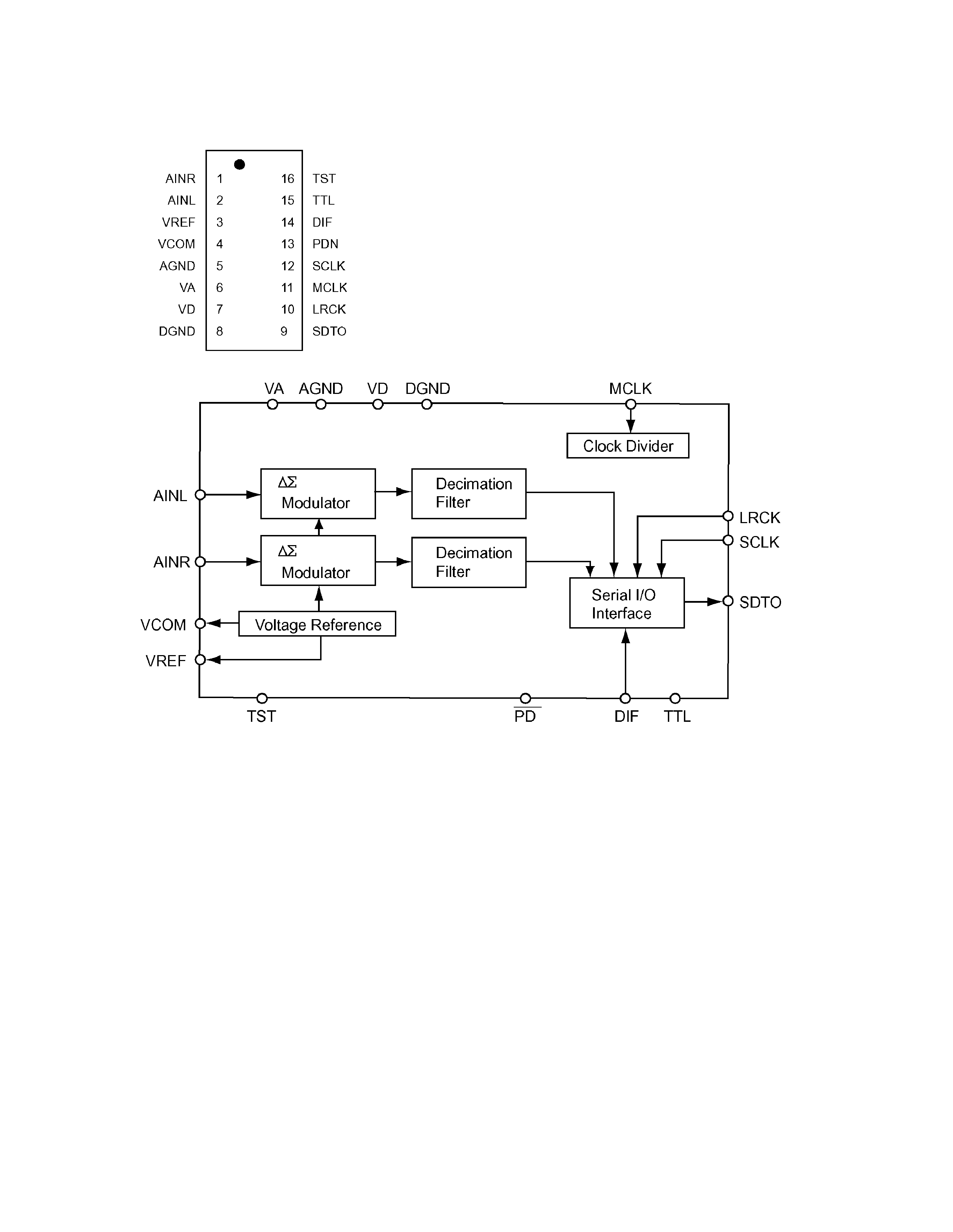
1.1 AK5353VT-X(IC511) : Converter
· Terminal layout
· Block diagram

XV-M52SL XV-M50BK
3
· Pin function
Note :
All input pins except pull-down pins should not be left floating.
No.
Pin name
I/O
Function
1
AINR
I
Rch Analog input pin
2
AINL
I
Lch Analog input pin
3
VREF
O Voltage Reference Output Pin
Normally connected to AGND with a 0.1µ F ceramic capacitor in parallel with an electrolytic
capacitor less than 4.7µ F.
4
VCOM
O Common Voltage Output Pin
Normally connected to AGND with a 0.1µ F ceramic capacitor in parallel with an electrolytic
capacitor less than 4.7µ F.
5
AGND
-
Analog Ground Pin, 0V
6
VA
-
Analog Power Supply Pin, +2.7~+5.5V
7
VD
-
Digital Power Supply Pin, +2.7~+5.5V
8
DGND
-
Digital Ground Pin, 0V
9
SDTO
O Serial Data Output Pin
Data bits are presented MSB first, in 2's complement format.
This pin is "L" in the power-down mode.
10
LRCK
I
Left/Right Channel Select pin
The fs clock is input to this pin.
11
MCLK
I
Master Clock Input Pin
12
SCLK
I
Serial Data Input Pin
Output data is clocked out on the falling edge of SCLK.
13
PDN
I
Power-Down Pin
When "L", the circuit is in power-down mode
The AK5353 should always be reset upon power-up.
14
DIF
I
Serial Interface Format Pin
L :MSB justified, "H": I2 S
15
TTL
I
Digital Input Level Select Pin
L : CMOS level (VA,VD = 2.7~5.5V), "H" : TTL level (VA,VD=4.5~5.5V)
16
TST
I
Test Pin (Internal pull-down pin)
This pin should be left floating.

XV-M52SL XV-M50BK
4
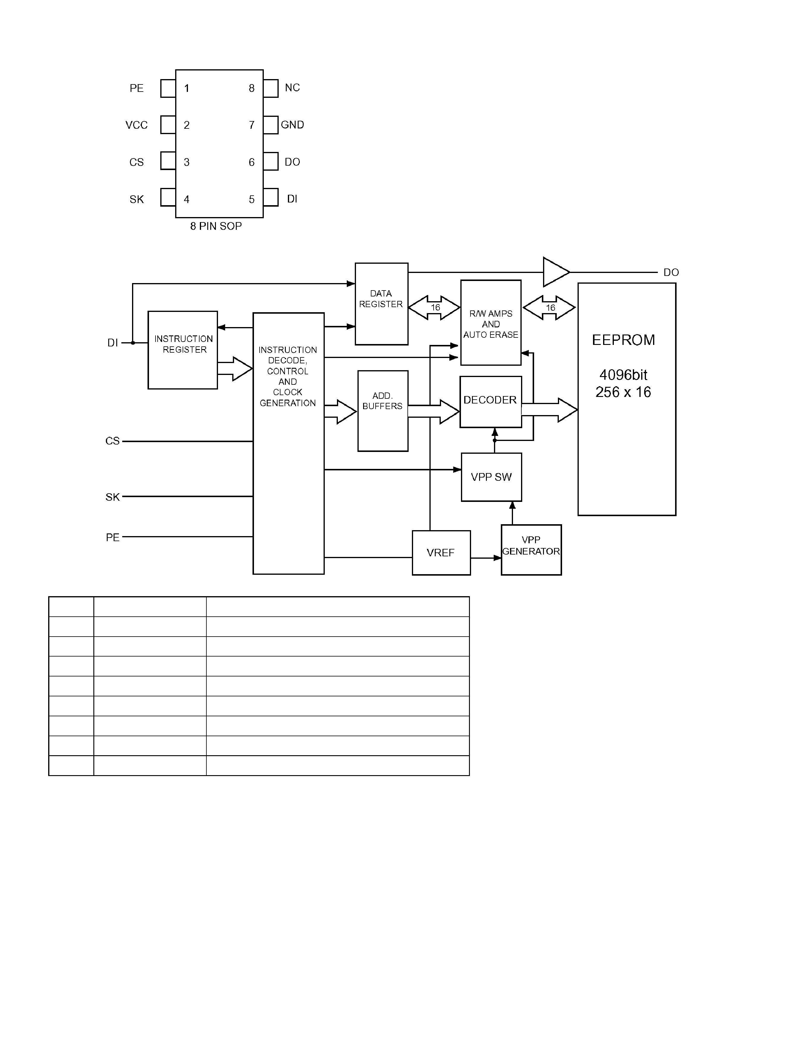
1.2 AK93C65AF-X (IC403) : EEPROM
· Pin layout
· Block diagram
· Pin function
NOTE :
The pull-up resistor of the PE pin is about 2.5Mohm (VCC=5V)
Pin no.
Symbol
Function
1
PE
Program enable (With built-in pull-up resistor)
2
VCC
Power supply
3
CS
Chip selection
4
SK
Cereal clock input
5
DI
Cereal data input
6
DO
Cereal data output
7
GND
Ground
8
NC
No connection

XV-M52SL XV-M50BK
5
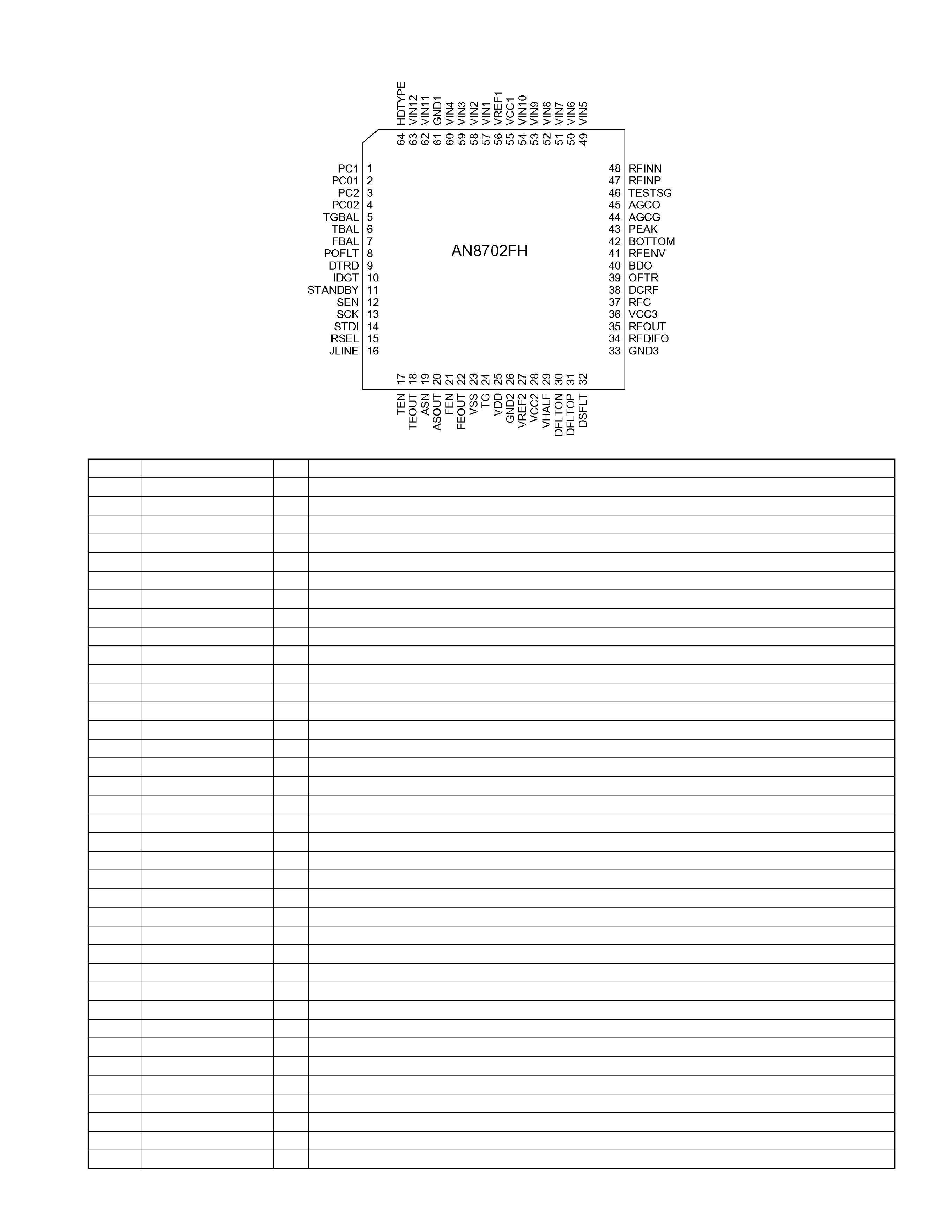
1.3 AN8702FH(IC101):Frontend processor
· Pin layout
· Pin function
Pin No.
Symbol
I/O
Description
1
PC1
I
Input for Laser current monitor
2
PC01
O Laser power control output for DVD
3
PC2
I
Photo detector fo CD
4
PC02
O Laser power control output for CD
5
TGBAL
I
Tangential phase balance control terminal
6
TBAL
I
Tracking balance control terminal
7
FBAL
I
Focus balance control ter
8
POFLT
O Track detection threshold level terminal
9
DTRD
I
Data slice part data read signal input terminal (For RAM)
10
IDGT
I
Data slice part address part gate signal input terminal (For RAM)
11
STANDBY
I
Standby mode control terminal
12
SEN
I
SEN(Serial data input terminal)
13
SCK
I
SCK(Serial data input terminal)
14
STDI
I
STDI(Serial data input terminal)
15
RSEL
I
DVD and CD selection
16
JLINE
I
J-line setting output (FEP)
17
TEN
I
Tracking error output amplifier reversing input terminal
18
TEOUT
O Tracking error signal output terminal
19
ASN
I
Off set adjustment terminal for DRC
20
ASOUT
O All added signal output terminal
21
FEN
I
Focus error output amplifier reversing input terminal
22
FEOUT
O Focus error signal output terminal
23
VSS
-
Connect to GND
24
TG
O Tangential phase error signal output terminal
25
VDD
-
Power supply terminal 3V
26
GND2
-
Connect to GND
27
VREF2
O VREF2 voltage output terminal
28
VCC2
-
Power supply terminal 5V
29
VHALF
O VHALF voltage output terminal
30
DFLTON
O Filter amplifier reversing output terminal
31
DFLTOP
O Filter amplifier output terminal
32
DSFLT
O Connected capacitor terminal for filter output
33
GND3
-
Connect to GND
34
RFDIFO
O RF operation output terminal
35
RFOUT
O RF output terminal
36
VCC3
-
Power supply terminal 5V
37
RFC
I
Filter for RF amplifier
