SERVICE MANUAL
SPECIFICATIONS AND PARTS ARE SUBJECT TO CHANGE FOR IMPROVEMENT
Digital Media Products Division,Tokai
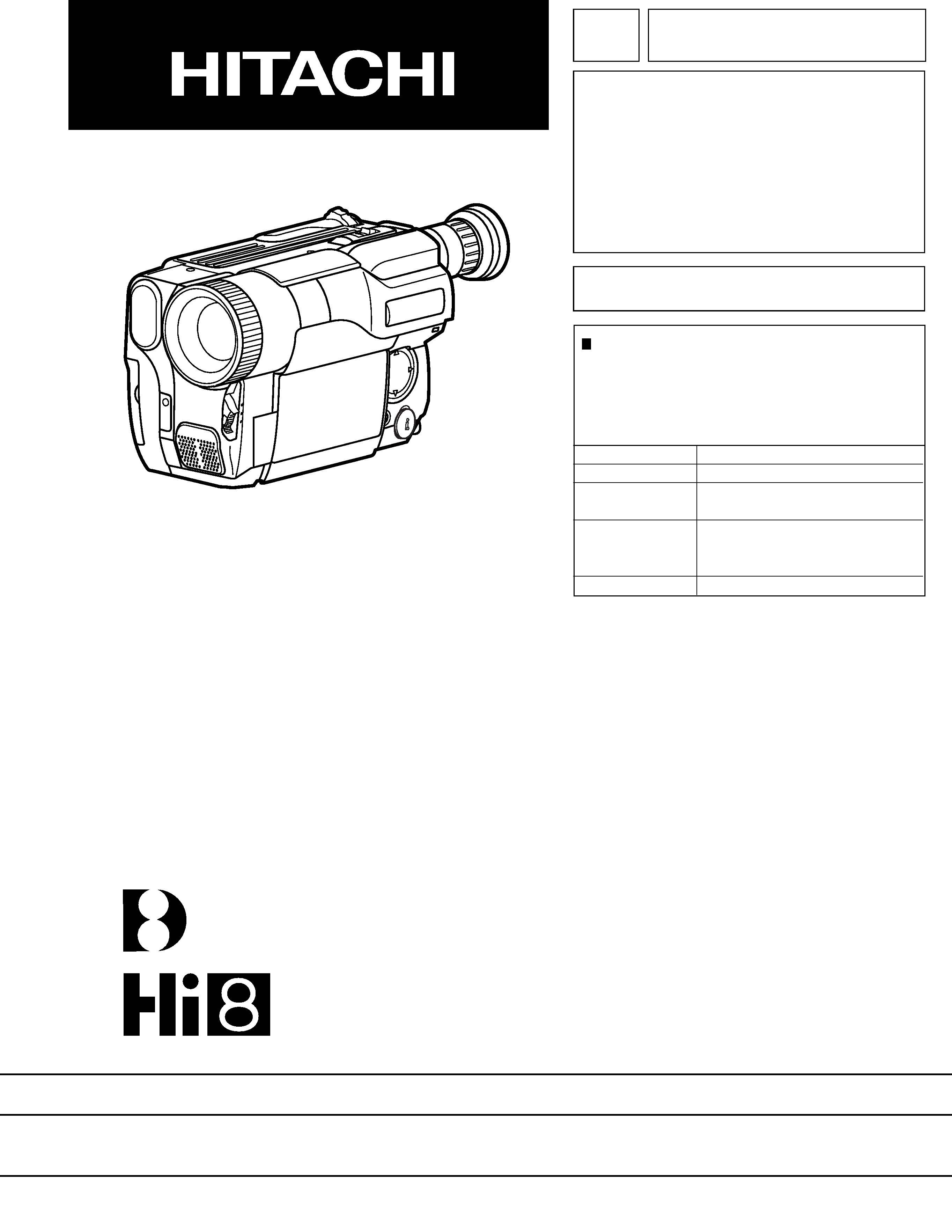
DIGITAL 8 VIDEO CAMERA/RECORDER
2001
May
TK
No. 7105E
VM-D975LA
VM-D875LA
VM-D873LA
UH MECHANISM
When Servicing the Mechanism:
This video camera/recorder uses a UH
mechanism.
When servicing the UH mechanism, refer to the
following service manuals:
Item
Manuals to be referred to
Disassembly
UH Mechanism (No. 6811E)
Mechanical
UH Mechanism Supplement
Adjustment
(No. 6811E-1)
Maintenance/
Inspection
UH mechanism (No. 6811E)
Procedure
Exploded View
Chapter 4 in this manual
AC Adapter
VM-ACE5A

CAUTION- 1
Many electrical and mechanical parts have special safety-related characteristics. These are often not evident from visual
inspection nor can the protection afforded by them necessarily be obtained by using replacement components rated for a
higher voltage, wattage, etc. Replacement parts which have these special safety characteristics are identified in this
Service Manual. Electrical components having such features are identified by marking with a
on the schematics and
the parts list in this Service Manual. The use of a substitute replacement component which does not have the same safety
characteristics as the HITACHI recommended replacement one, shown in the parts list in this Service Manual, may create
shock, fire, or other hazards. Product safety is continuously under review and new instructions are issued from time to time.
For the latest information, always consult the current HITACHI Service Manual. A subscription to, or additional copies for,
HITACHI Service Manual may be obtained at a nominal charge from HITACHI SALES CORPORATION.
TYPE identification
Model name
TYPE 975
VM-D975LA
TYPE 875
VM-D875LA
TYPE 873
VM-D873LA
How to discriminate the "TYPE" identifications in the manual
The parts and circuits are identified by "TYPE" in this manual to discriminate the differences between models. The
TYPE numbers are the same as the model numbers. The table below shows how to read the type identifications.
CAUTION (COLOR LCD)
LCD display; the liquid crystal display (LCD) panel is mode by highly precise technology.
More than 99.99% of its picture elements (pixels) are effective, but some (less than 0.01%) may appear as colored
bright dots. This mode not indicate a fault as the LCD panel stretches the limits of current technology.
Be careful of the section painted in white on the electronic viewfinder circuit board as it generates a high voltage.
The primary source of X-ray radiation in this viewfinder is the picture tube. The tube used in this viewfinder is specially
constructed to limit X-ray radiation emission. For continued X-ray radiation protection, the replacement tube must be
same type as the original, Hitachi approved one.
CAUTION (CRT EVF)
PRODUCT SAFETY NOTICE
X-RAY RADIATION
!
Cautions
Microsoft, MS, MS-DOS, Windows and Windows NT are registered trademarks of Microsoft Corporation.
Pentium and Celeron are registered trademarks of Intel Corporation.
Manufactured under license from Dolby Laboratories.
"Dolby" and double-D symbol are trademarks of Dolby Laboratories.
Confidential unpublished works. (C) 1992-2000 Dolby Laboratories Inc. All rights reserved.
IBM is registered trademarks of International Business Machines Corporations.
Other company names and product names listed are trademarks or brand names belonging to each company.

CAUTION- 2
Notes When Using Service Manual
The following shows the contents to be noted when using service manual:
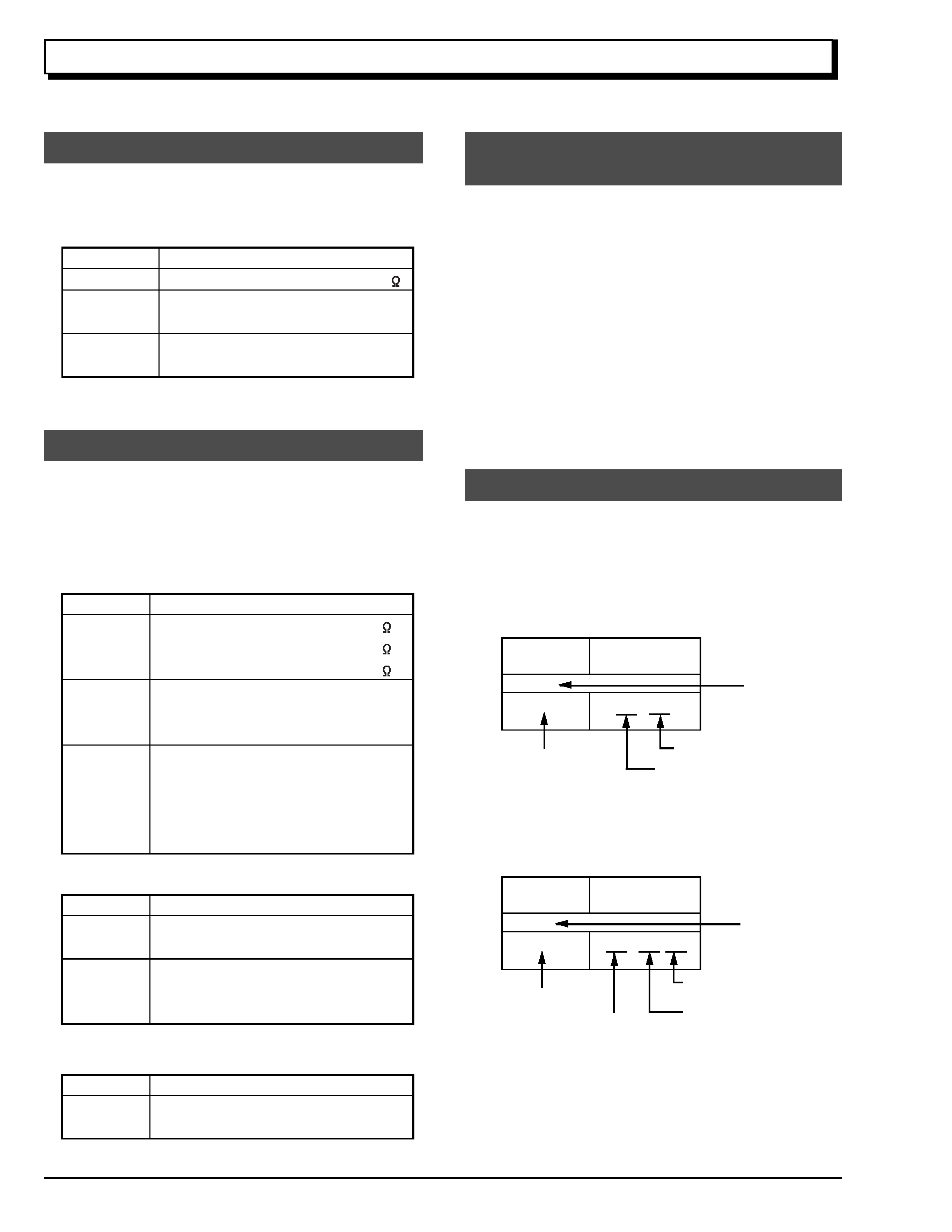
1. Value units used in parts list
This table shows locations of each part on circuit board
diagrams. The locations are indicated using the guide
scales on the external lines of diagrams.
1) One diagram indicated for each board
The values, dielectric strength (power capacitance) and
tolerances of the resistors (excluding variable resistors)
and capacitors are indicated in the schematic diagrams
using abbreviations.
[Resistors]
Certain symbols are indicated below for value units of
resistors, capacitors and coils in parts list. When you read
them note the following regular indications:
Indication in list
Regular indication
KOHM ........................................... k
UF ................................................ µF
PF ................................................ pF
UH ................................................ µH
MH ............................................... mH
Parts
Resistor
Capacitor
Coil
2) Two diagrams indicated for each board
2. Values in schematic diagrams
Item
Value
Tolerance
Power
capacitance
Indication
No indication ...................................
K ................................................... k
M .................................................. M
No indication ............................. ±5%
(All tolerances other than ±5% are
indicated in schematic diagrams)
No indication ............................ 1/8W
(1/16W for leadless resistors without
indication)
All capacitances other than the above
are indicated in schematic diagrams.
[Capaci-
tors]
Item
Value
Dielectric
strength
Indication
No indication ................................. µF
P ................................................... pF
No indication .............................. 50V
(All dielectric strengths other than 50V
are indicated in schematic diagrams)
Item
Value
Indication
µ .................................................... µH
m .................................................. mH
[Coils]
3. Identifications of sides A/B in
circuit board diagrams
1) Board having a pattern on one side and parts on both
sides.
Side A: Shows discrete parts, viewed from the pattern
side.
Side B: Shows leadless parts, viewed from the
pattern side.
2) Board having patterns on both sides and parts on
both sides.
Side A: Shows parts and patterns which can be seen
when the case is opened.
Side B: Shows parts and the pattern on the back of
side A.
4. Table for indexing locations of parts
Parts
Location
2
A
Symbol
No.
IC
IC1201
Type of part
Zone "A" on board diagram
Circuit No.
Zone "2" on board diagram
Parts
Location
A - 2
A
Symbol
No.
IC
IC1201
Zone "2" on board
diagram
A: Shows side A
B: Shows side B
Zone "A" on board
diagram
Type of
part
Circuit No.

CAUTION- 3
Before Servicing (Before Initializing EEPROM)
CAUTION:
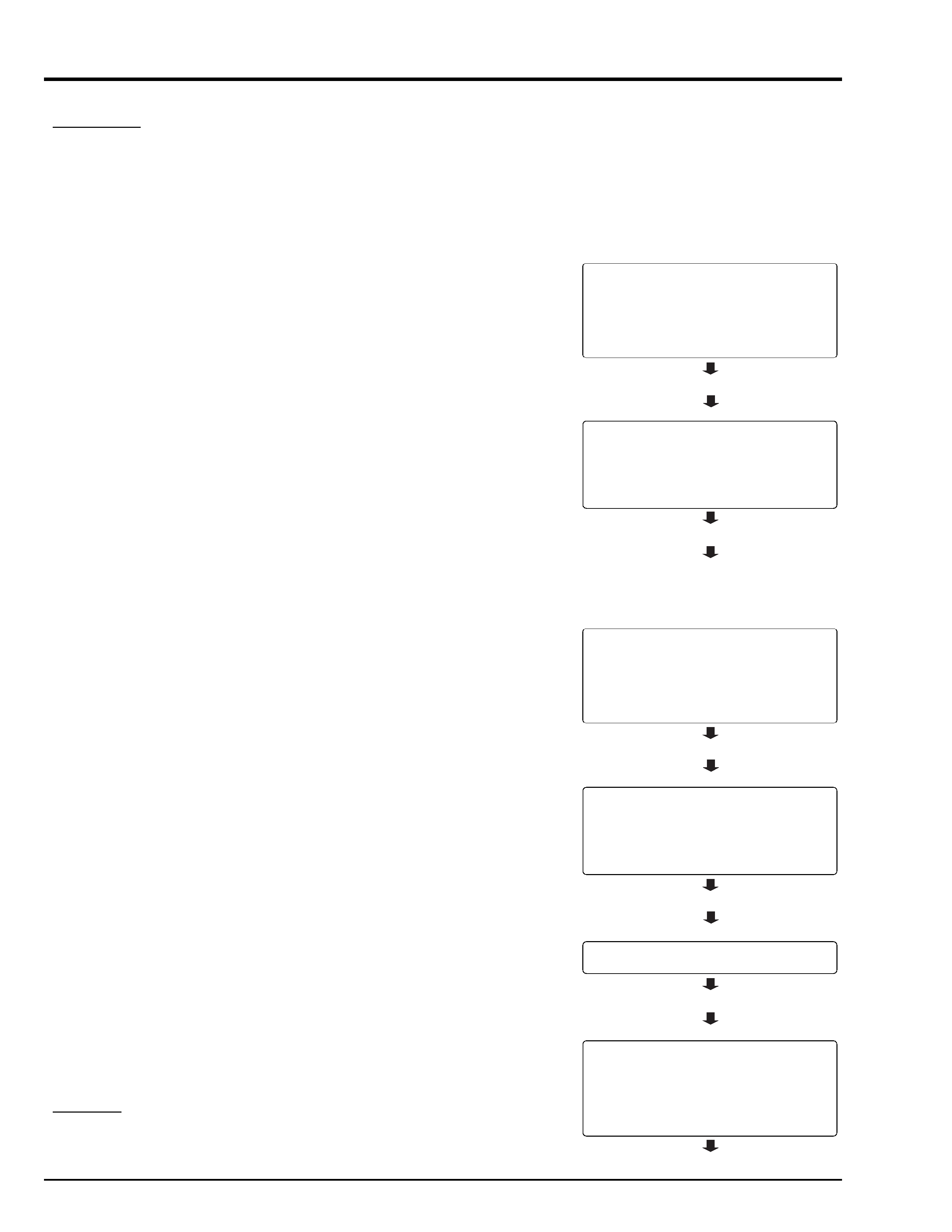
Before servicing this video camera/recorder (before initializing EEPROM),
check the IEEE1394 ID No. by the following procedure:
Be sure to input the IEEE1394 ID No. after initializing the EEPROM.
Before Starting Check Method or Input:
(1) Connect the video camera/recorder, personal computer, power supply, etc. in
the same way as for adjustment, referring to Fig. 2-1 in Chapter 3 (see
page 3-2).
(2) Start the MAP (manual adjustment program for service), referring to
"4. Starting Adjustment Program (MAP)" in Chapter 3 (see page 3-5).
(3) Input A to PC on the main menu screen to display the data maintenance
menu screen. (For "DATA INITIALIZE", see "5.1 Data Maintenance" in
Chapter 3.)
(4) Input 2 to PC on the data maintenance menu screen to display the IEEE1394
ID maintenance menu screen.
Main menu
***********************************************************
MANUAL ADJUSTMENT PROGRAM
***********************************************************
[A]
DATA MAINTENANCE
[B]
ADJUSTMENT
[C]
AUTO FOCUS
[D]
VCR ADJUSTMENT
[E]
STABILIZER
[F]
SPOT NOISE
[G]
LCD
[H]
COLOR EVF
[ESC] END
Please select [A] - [H] or [ESC]
Input A.
***********************************************************
DATA MAINTENANCE
***********************************************************
[1]
DATA INITIALIZE
[2]
IEEE1394 MAINTENANCE
[ESC] RETURN TO MAIN MENU
Please select [1] - [2] or [ESC]
Data maintenance menu
IEEE1394 ID maintenance menu
***********************************************************
IEEE1394 ID MAINTENANCE
***********************************************************
[1]
LOAD CURRENT CHIP_ID
[2]
REWRITE CHIP_ID
[3]
WRITE CHIP_ID
[ESC] RETURN TO MAIN MENU
Please select [1] - [3] or [ESC]
Input 1.
IEEE1394 ID No.
Make a note of ID No.
Press any key.
1.
IEEE1394 ID No. Check Method
(1) Input 1 to PC on the IEEE1394 ID maintenance menu screen.
(2) The IEEE1394 ID No. screen will appear: Make a note of it.
(3) Press any key to restore the IEEE1394 ID maintenance menu screen.
IMPORTANT:
If the IEEE1394 ID No. cannot be confirmed by the above procedure because of
some defect in EEPROM, etc., a new ID No.
will be necessary. Obtain the new ID No., referring to "3. Method for Obtaining
New ID No.", and input it, referring to "2.2 Entering new ID No.".
Input 2.
IEEE1394 ID maintenance menu
***********************************************************
IEEE1394 ID MAINTENANCE
***********************************************************
[1]
LOAD CURRENT CHIP_ID
[2]
REWRITE CHIP_ID
[3]
WRITE CHIP_ID
[ESC] RETURN TO MAIN MENU
Please select [1] - [3] or [ESC]
<< CURRENT CHIP_ID DATA LOADING >>
CHIP_ID H= 00
CHIP_ID L= 00 00 00 00
PRESS ANY KEY

CAUTION- 4
2.
IEEE1394 ID No. Input Method
IMPORTANT:
Be sure to perform this task after initializing the EEPROM.
If ID No. is to be input after EEPROM (or VCA circuit board) is replaced and new
EEPROM is initialized, use the ID No. that has already been checked. (It is not
necessary to obtain a new ID No.)
2.1
Entering checked ID No.
The following is the procedure for entering the ID No. checked in "1. IEEE1394 ID
No. Check Method": Normally, use this procedure.
(1) Input 2 to PC on the IEEE1394 ID maintenance menu screen to display the
ID rewrite screen.
(2) Enter the 2-digit ID No. for the CHIP ID H item and press the Enter key.
(3) Enter the 8-digit ID No. for the CHIP ID L item: Input 2 digits at a time starting
from the left, and press the Enter key for each 2-digit input.
(4) Press the Enter key to restore IEEE1394 ID maintenance menu screen.
(5) Perform the procedure in "1. IEEE1394 ID No. Check Method" to make sure
that the ID No. has been entered correctly.
IEEE1394 ID maintenance menu
***********************************************************
IEEE1394 ID MAINTENANCE
***********************************************************
[1]
LOAD CURRENT CHIP_ID
[2]
REWRITE CHIP_ID
[3]
WRITE CHIP_ID
[ESC] RETURN TO MAIN MENU
Please select [1] - [3] or [ESC]
Input 2.
ID No. rewrite
<< CURRENT CHIP_ID DATA >>
CHIP_ID H= 00
CHIP_ID L= 00 00 00 00
<< INPUT CHIP_ID DATA >>
CHIP_ID_H ---->
Enter the ID No.
Press the Enter key.
2.2
Entering a new ID No.
Perform this section only when the ID No. cannot be checked by the procedure in
"IEEE1394 ID No. Check Method" because of a defect in EEPROM. Normally,
refer to "2.1 Entering checked ID No.".
Refer to "3. Method for Obtaining New ID No." for how to obtain new ID No. to be
entered by the following procedure:
(1) Input 3 to PC on the IEEE1394 ID maintenance menu screen.
(2) The screen for verifying the new ID No. input will appear: Input Y to PC.
(3) The new ID No. input screen will appear.
(4) Enter the new 2-digit ID No. for the CHIP ID H item and press the Enter key.
(5) Enter the new 8-digit ID No. for the CHIP ID L item: Input 2 digits at a time
starting the left, and press the Enter key for each 2-digit input.
(6) The new ID No. input complete screen will appear.
(7) Press the Enter key to restore IEEE1394 ID maintenance menu screen.
(8) Perform the procedure in "1. IEEE1394 ID No. Check Method" to make sure
that the new ID No. has been entered correctly.
3.
Method for Obtaining New ID No.
If the ID No. cannot be confirmed by the procedure in "1. IEEE1394 ID No. Check
Method", a new ID No. will be necessary. Obtain the new ID No. using the follow-
ing procedure:
The details on the method for obtaining the new ID No. will be given later.
CAUTION:
If the ID No. can be confirmed by the procedure in "1. IEEE1394 ID No. Check
Method", be sure not to attempt to obtain a new ID No.
IEEE1394 ID maintenance menu
***********************************************************
IEEE1394 ID MAINTENANCE
***********************************************************
[1]
LOAD CURRENT CHIP_ID
[2]
REWRITE CHIP_ID
[3]
WRITE CHIP_ID
[ESC] RETURN TO MAIN MENU
Please select [1] - [3] or [ESC]
Input 3.
Verifying the new ID No. input
<< NEW CHIP_ID DATA >>
CHIP_ID H= 00
CHIP_ID L= 00 00 00 00
<< DATA WRITING >>
START TO SEND DATA. (Y/N)
Input Y.
<< INPUT NEW CHIP_ID DATA >>
CHIP_ID_H ----> 00
New ID No. input
Enter the new ID No.
Press the Enter key.
New ID No. input complete
<< NEW CHIP_ID DATA >>
CHIP_ID H= 00
CHIP_ID L= 00 00 00 00
<< DATA WRITING >>
FINISHED WRITING DATA
PRESS ANY KEY
