RN-9437G-A,B
- 1 -
Service Manual
Published by Service Dept.
Printed in Japan
Clarion Co., Ltd.
7-2, Shintoshin, Chuo-ku, Saitama-shi, Saitama 330-0081 Japan
Service Dept.: 7-2, Shintoshin, Chuo-ku, Saitama-shi, Saitama 330-0081 Japan
Tel: +81-48-601-3705 FAX: +81-48-601-3804
298-6535-00 Jan.2008
Model
CB02A
NISSAN MOTOR Genuine
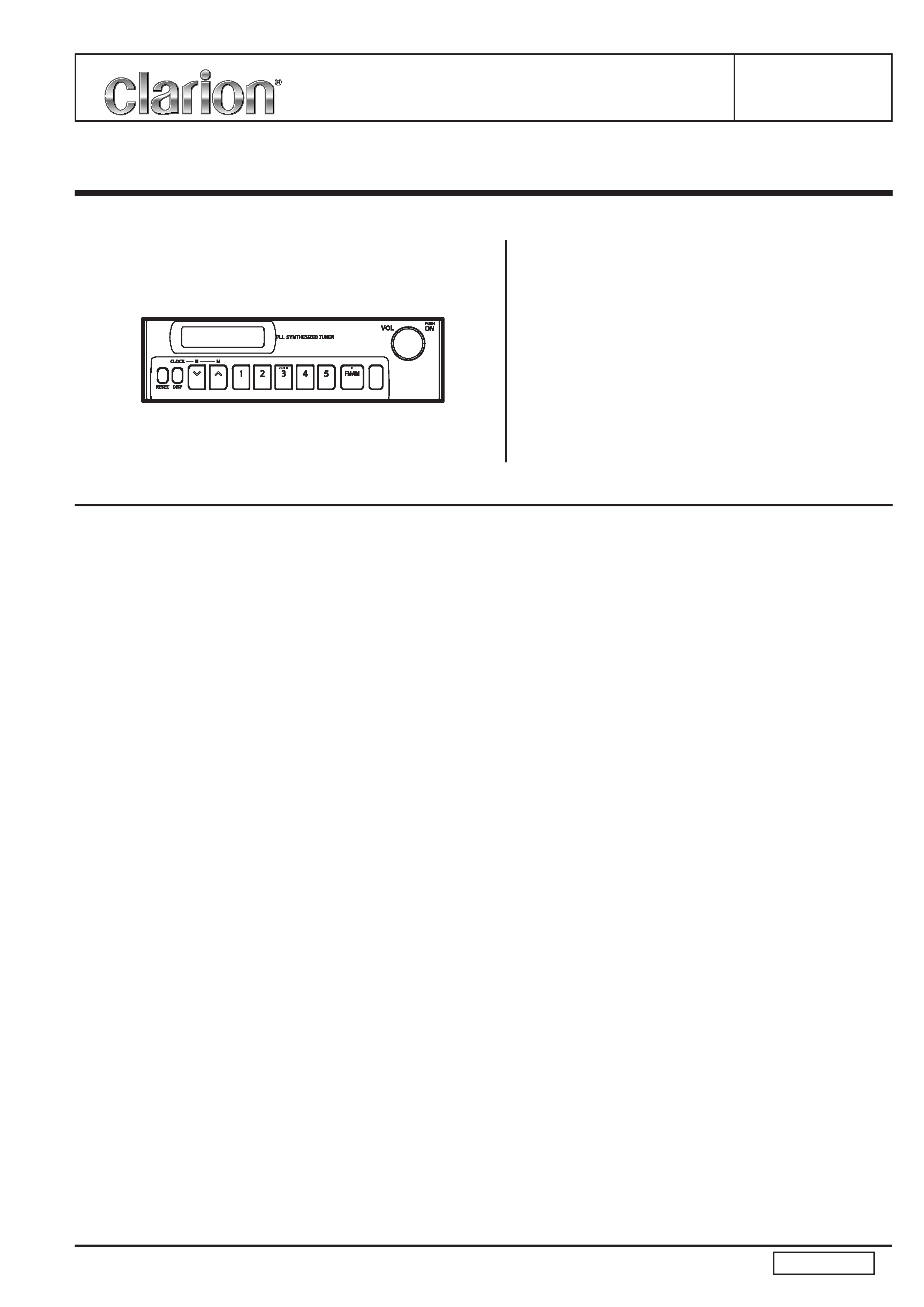
AM/FM RADIO
RN-9437G-A,B
(Genuine No.28013 VZ10A)
ID No.CB02A
SPECIFICATIONS
Radio section
Tuning system:
PLL Frequency synthesizer system
AM Receive range:
531kHz to 1,602kHz
9 kHz step
530kHz to 1,620kHz
10 kHz step
FM Receive range:
87.5MHz to 107.9MHz
50 kHz step
Intermediate frequency:
AM 450 +3/-3 MHz
FM 10.7 +0.2/-0.2 MHz
Quieting sensitivity:
AM Less than 32dBu (at 20dB S/N)
FM Less than 10dBu (at 30dB S/N)
Separation:
FM 22 +5/-7 dB (at 1kHz)
Auto tuning stop sensitivity:
AM 32 +6/-6 dBu(at DX)
FM 25 +6/-6 dBu
Load impedance:
4 ohm
Power supply voltage: DC13.2V(10.8 to 15.6V)
Negative ground
Current consumption: Less than 5A
Dimensions(mm):
178(W) x50(H) x143(D)
Weight:
0.7kg
Setting the reception area
1. While pressing the CH3 and CH4 button,press the UP
button to change the AM Receiving area from 9 kHz step
to 10 kHz step.
NOTE
*
There are two models with a different production place.
China production : RN-9437G-A
Malaysia production: RN-9437G-B
All the same parts are used and assemble these mod-
els.
*
We cannot supply PWB with component parts in prin-
ciple. When a circuit on PWB has failure, please repair it
by component parts base. Parts which are not mentioned
in service manual are not supplied.
*
Specifications and design are subject to change without
notice for further improvement.
COMPONENTS
RN-9437G-A,B
Main unit
---------
1
To engineers in charge of repair or
inspection of our products.
Before repair or inspection, make sure to follow the
instructions so that customers and Engineers in charge
of repair or inspection can avoid suffering any risk or
injury.
1. Use specified parts.
The system uses parts with special safety features against fire
and voltage. Use only parts with equivalent characteristics
when replacing them.
The use of unspecified parts shall be regarded as remodeling
for which we shall not be liable. The onus of product liability
(PL) shall not be our responsibility in cases where an accident
or failure is as a result of unspecified parts being used.
2. Place the parts and wiring back in their original positions after
replacement or re-wiring.
For proper circuit construction, use of insulation tubes, bond-
ing, gaps to PWB, etc, is involved. The wiring connection and
routing to the PWB are specially planned using clamps to keep
away from heated and high voltage parts. Ensure that they are
placed back in their original positions after repair or inspec-
tion.
RN-9437G-A,B
- 2 -
If extended damage is caused due to negligence during re-
pair, the legal responsibility shall be with the repairing com-
pany.
3. Check for safety after repair.
Check that the screws, parts and wires are put back securely
in their original position after repair. Ensure for safety reasons
there is no possibility of secondary ploblems around the re-
paired spots.
If extended damage is caused due to negligence of repair, the
legal responsibility shall be with the repairing company.
4. Caution in removal and making wiring connection to the parts
for the automobile.
Disconnect the battery terminal after turning the ignition key
off. If wrong wiring connections are made with the battery con-
nected, a short circuit and/or fire may occur. If extensive dam-
age is caused due to negligence of repair, the legal responsi-
bility shall be with the repairing company.
5. Cautions in soldering
Please do not spread liquid flux in soldering.
Please do not wash the soldering point after soldering.
6. Cautions in soldering for chip capacitors
Please solder the chip capacitors after pre-heating for replace-
ment because they are very weak to heat.
Please do not heat the chip capacitors with a soldering iron
directly.
7. Cautions in handling for chip parts.
Do not reuse removed chips even when no abnormality is ob-
served in their appearance. Always replace them with new
ones. (The chip parts include resistors, capacitors, diodes, tran-
sistors, etc).
Please make an operation test after replacement.
8. Cautions in handling flexible PWB
Before working with a soldering iron, make sure that the iron
tip temperature is around 270
. Take care not to apply the
iron tip repeatedly(more than three times)to the same patterns.
Also take care not to apply the tip with force.
9. Turn the unit OFF during disassembly and parts replacement.
Recheck all work before you apply power to the unit.
880-1921B
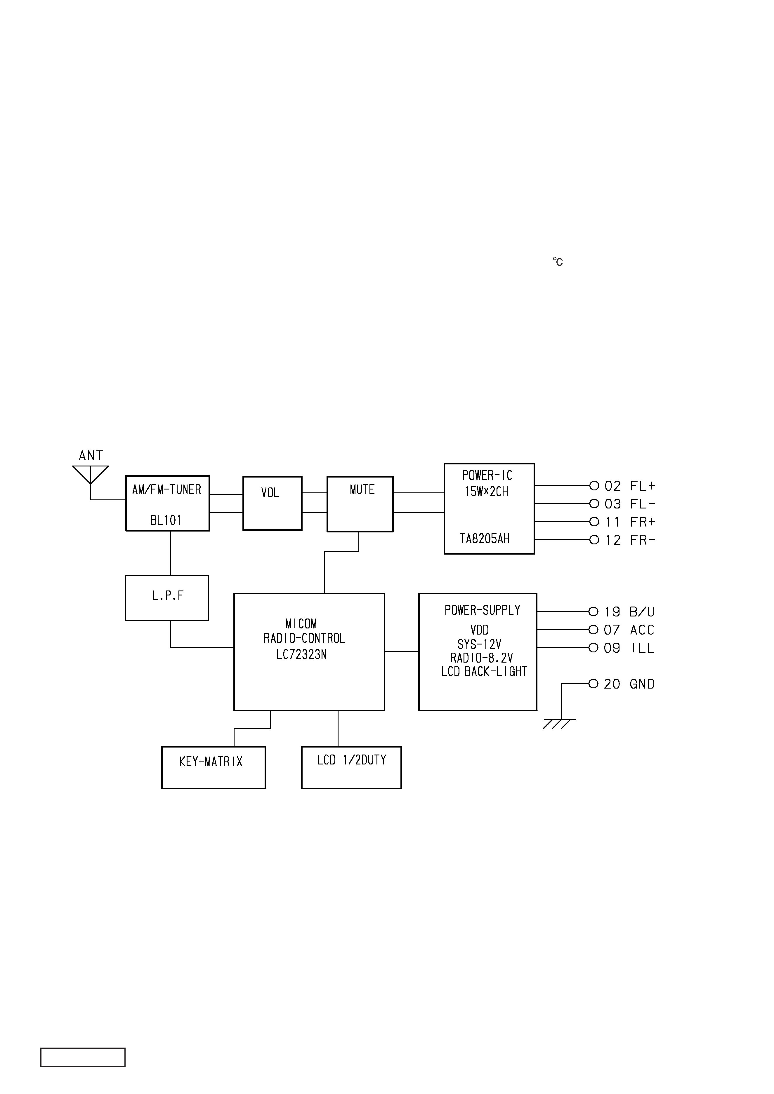
Q103,104
VR101
Q301,302
IC301
IC401
LCD701
S701-710
BLOCK DIAGRAM
RN-9437G-A,B
- 3 -
ADJUSTMENT
Item
Procedure
Measuring instrument
FM noise
convergence
1.Input the 98.1MHz/55dBu(400Hz 22.5kHz Div.) SSG signal.
2.Set the output to 0dBm(0.775V)by main volume.
3.Adjust VR102 so that the output level is -18 +3/-3 dB when the output of SSG is
set to -20dBu.
SSG
Milli-volt meter
Clock accuracy
1.Connect the Choronometer to TP201.
2.Adjust TC401 so that an output of TP201 becomes 0.0 +1.0/-0.0Sec./day.
Choronometer
EXPLANATION OF IC
052-1131-20
LC72323N-9055E
System Controller
Terminal Description
pin
1: X IN
: IN : Crystal connection.
pin
2: TEST
2
: IN : For the test.
pin
3: ILL ON
: IN : Illumination ON signal input.
pin
4: NC
: IN : Not in use.
pin
5: NC
: IN : Not in use.
pin
6: NC
: IN : Not in use.
pin
7: SYS ON
: O : System ON signal output.
pin
8: NC
: O : Not in use.
pin
9: AM ON
: O : AM ON signal output.
pin 10: FM ON
: O : FM ON signal output.
pin 11: ST/TW/SD
:I/O: AM station receiving:
This port outputs a pulse by AM 900kHz
receiving.
FM station receiving:
This port detects the stereo signal. And
at seeking or scanning, this port detects
the SD signal.
pin 12: RF MUTE
: O : Radio frequency signal muting.
pin 13: DX/LO
: O : DX/Local select signal output.
pin 14: POWER SW
: IN : Power switch ON signal input.
pin 15: ANT ON
: O : Antenna ON command output.
pin 16: AMP ON
: O : Audio power amplifier ON signal output.
pin 17: AF MUTE
: O : Audio frequency signal muting.
pin 18: NC
: IN : Not in use.
pin 19: NC
: O : Not in use.
pin 20: NC
: O : Not in use.
pin 21: NC
: O : Not in use.
pin 22: NC
: O : Not in use.
pin 23: NC
: O : Not in use.
pin 24: NC
: O : Not in use.
pin 25: NC
: O : Not in use.
pin 26: NC
: O : Not in use.
pin 27: KS out 3
: O : Key scan output.
pin 28: KS out 2
: O : Key scan output.
pin 29: KS out 1
: O : Key scan output.
pin 30: KS out 0
: O : Key scan output.
pin 31: VDD
: - : Positive voltage supply.
pin 32: KS IN
0
: IN : Key scan input.
pin 33: KS IN
1
: IN : Key scan input.
pin 34: KS IN
2
: IN : Key scan input.
pin 35: KS IN
3
: IN : Key scan input.
pin 36: BACK LIGHT
: O : The back light ON signal output.
pin 37: NC
: O : Not in use.
pin 38: NC
: O : Not in use.
pin 39: NC
: O : Not in use.
pin 40: NC
: O : Not in use..
pin 41: NC
: O : Not in use.
pin 42: NC
: O : Not in use.
pin 43: NC
: O : Not in use.
pin 44: Seg out 20
: O : The segment signal output.
pin 45: Seg out 19
: O : The segment signal output.
pin 46: Seg out 18
: O : The segment signal output.
pin 47: Seg out 17
: O : The segment signal output.
pin 48: Seg out 16
: O : The segment signal output.
pin 49: Seg out 15
: O : The segment signal output.
pin 50: Seg out 14
: O : The segment signal output.
pin 51: Seg out 13
: O : The segment signal output.
pin 52: Seg out 12
: O : The segment signal output.
pin 53: Seg out 11
: O : The segment signal output.
pin 54: Seg out 10
: O : The segment signal output.
pin 55: Seg out
9
: O : The segment signal output.
pin 56: Seg out
8
: O : The segment signal output.
pin 57: Seg out
7
: O : The segment signal output.
pin 58: Seg out
6
: O : The segment signal output.
pin 59: Seg out
5
: O : The segment signal output.
pin 60: Seg out
4
: O : The segment signal output.
pin 61: Seg out
3
: O : The segment signal output.
pin 62: Seg out
2
: O : The segment signal output.
pin 63: Seg out
1
: O : The segment signal output.
pin 64: Common 2
: O : The common signal output.
pin 65: Common 1
: O : The common signal output.
pin 66: INT IN
: IN : Interruption demand.
pin 67: HOLD
: IN : ACC ON signal input.
pin 68: RESET
: IN : Reset signal input.
pin 69: NC
: IN : Not in use.
pin 70: FM IF IN
: IN : The input terminal of the internal counter
for FM IF.
pin 71: AM IF IN
: IN : The input terminal of the internal counter
for AM IF.
pin 72: SNS
: IN : The backup voltage fail down detection.
pin 73: VDD
: - : Positive voltage supply.
pin 74: FM OSC IN
: IN : The input terminal of the internal counter
for FM OSC ( Local Oscillation ).
pin 75: AM OSC IN
: IN : The input terminal of the internal counter
for AM OSC ( Local Oscillation ).
pin 76: VSS
: - : Negative voltage supply.
pin 77: ERROR 1
: O : PLL error signal output.
pin 78: ERROR 2
: O : PLL error signal output.
pin 79: TEST
1
: IN : For the test.
pin 80: X out
: O : Crystal connection.
RN-9437G-A,B
- 4 -
5
6
7
8
11
12
1-1
1
2
13
33
13
4
E
F
G
H
32
31
30
32
29 34
23
24
28
19
20
16
21
26
27
18
18
19
20
22
35
17
15
H
E
14
10
9
3
25
G
F
16
16
36
1
940-8074-21
ESCUTCHEON ASSY
1
1-1
716-0872-51
PAD SCREW (M1.7X6)
3
2
380-5597-00
KNOB
1
3
311-1892-01
LOWER CASE
1
4
310-1796-00
UPPER CASE
1
5
331-3825-00
LCD COVER
1
6
379-1312-20
INDICATOR (LCD)
1
7
335-5317-00
COLOR FILTER
1
8
335-7264-00
LCD HOLDER
1
9
335-7263-00
LAMP HOUSE
1
10
074-1012-03
OUTLET SOCKET
1
11
345-3842-15
LAMP CAP
1
12
017-0394-00
PILOT LAMP
1
13
714-2606-8B MACHINE SCREW (M2.6X6)
4
14
722-0370-51
NUT(M9)
1
15
309-0800-01
FRONT PLATE
1
16
---------------
MAIN PWB
1
17
013-6005-51
SWITCH
10
18
017-0440-12
PILOT LAMP
3
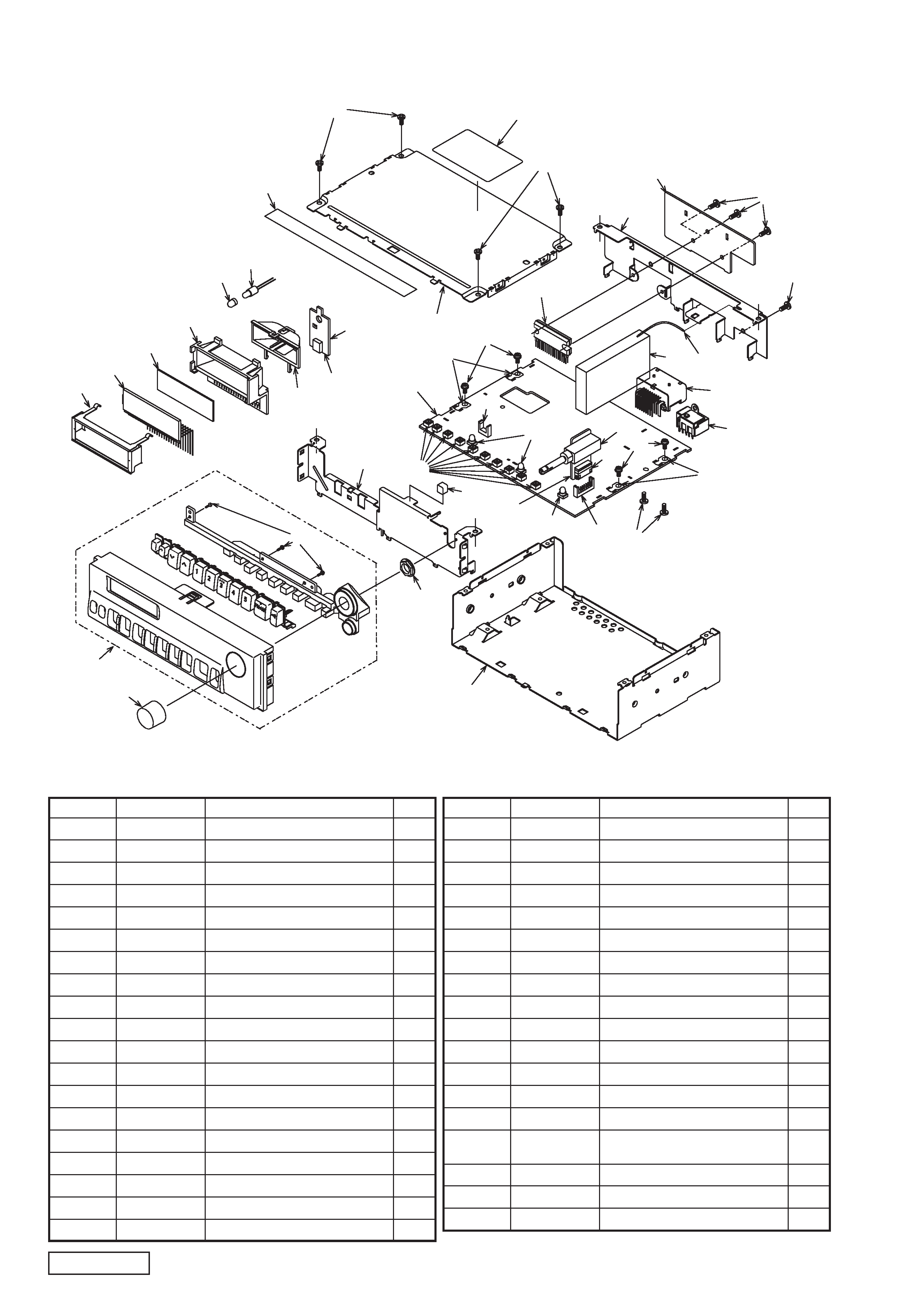
EXPLODED VIEW/PARTS LIST
Main section
19
716-0878-50
IT SCREW (M2.6X5)
4
20
073-0768-90
TERMINAL
4
21
076-0454-03
PLUG
1
22
051-0958-01
IC (TA8205AH)
1
23
074-4009-20
OUTLET SOCKET
1
24
092-2210-01
ANT-RECEPT
1
25
778-3006-00
TAP SCREW
2
26
074-1012-07
OUTLET SOCKET
1
27
076-0454-07
PLUG
1
28
016-2000-04
VARIABLE RESISTOR
1
29
880-1921B
AM/FM TUNER
1
30
307-0705-00
REAR PLATE
1
31
313-1679-00
HEAT SINK
1
32
714-2608-8B MACHINE SCREW(M2.6X8)
4
33
286-6510-05
SETPLATE(37G-A)
1
286-6671-13
SETPLATE(37G-B)
34
800-0204-00
VINYL COAT WIRE
1
35
345-6066-00
GASKET
1
36
353-0522-10
SHADE
1
NO.
PART NO.
DESCRIPTION
Q'TY
NO.
PART NO.
DESCRIPTION
Q'TY
Note)Some parts depend on each model.The model name is specified in the descripion .
(37G-A;RN-9437G-A, 37G-B;RN-9437G-B)
RN-9437G-A,B
- 5 -
R115
119-1021-15 1/10W 1k ohm
R116
119-1051-15 1/10W 1M ohm
R117
119-0000-05 1/10W 0 ohm JW
R201
119-4711-15 1/10W 470 ohm
R202
119-4711-15 1/10W 470 ohm
R203
119-6821-15 1/10W 6.8k ohm
R204
119-2731-15 1/10W 27k ohm
R205
119-2731-15 1/10W 27k ohm
R206
119-6821-15 1/10W 6.8k ohm
R207
119-0000-05 1/10W 0 ohm JW
R208
119-0000-05 1/10W 0 ohm JW
R209
119-0000-05 1/10W 0 ohm JW
R210
119-0000-05 1/10W 0 ohm JW
R211
119-4721-15 1/10W 4.7k ohm
R212
119-4721-15 1/10W 4.7k ohm
R213
119-0000-05 1/10W 0 ohm JW
R214
119-0000-05 1/10W 0 ohm JW
R217
119-2221-15 1/10W 2.2k ohm
R218
119-2221-15 1/10W 2.2k ohm
R301
119-6821-15 1/10W 6.8k ohm
R302
119-6821-15 1/10W 6.8k ohm
R303
119-1031-15 1/10W 10k ohm
R304
119-1031-15 1/10W 10k ohm
R305
119-1031-15 1/10W 10k ohm
R306
119-1021-15 1/10W 1k ohm
R307
119-4711-15 1/10W 470 ohm
R308
119-4711-15 1/10W 470 ohm
R309
119-2291-15 1/10W 2.2 ohm
R310
119-2291-15 1/10W 2.2 ohm
R311
119-2291-15 1/10W 2.2 ohm
R312
119-2291-15 1/10W 2.2 ohm
R401
119-4731-15 1/10W 47k ohm
R402
119-4731-15 1/10W 47k ohm
R403
119-4731-15 1/10W 47k ohm
R411
119-2221-15 1/10W 2.2k ohm
R412
119-2231-15 1/10W 22k ohm
R413
119-2231-15 1/10W 22k ohm
R504
116-3311-15 1/4W 330 ohm
R505
119-4721-15 1/10W 4.7k ohm
R506
119-2231-15 1/10W 22k ohm
R509
119-1031-15 1/10W 10k ohm
R510
119-5611-15 1/10W 560 ohm
R511
116-1531-15 1/4W 15k ohm
R512
116-2721-15 1/4W 2.7k ohm
R602
116-1221-15 1/4W 1.2k ohm
R603
114-1201-18 1W 12 ohm
R604
116-1221-15 1/4W 1.2k ohm
S701
013-6005-51 SKQNAB
S702
013-6005-51 SKQNAB
S703
013-6005-51 SKQNAB
S704
013-6005-51 SKQNAB
S705
013-6005-51 SKQNAB
S706
013-6005-51 SKQNAB
S707
013-6005-51 SKQNAB
S708
013-6005-51 SKQNAB
S709
013-6005-51 SKQNAB
S710
013-6005-51 SKQNAB
SUP101 060-0122-91 DSP-141N-S00B
TC401
004-1580-64 47pF
TM101
073-0768-90 TERMINAL
TM102
073-0768-90 TERMINAL
TM103
073-0768-90 TERMINAL
TM104
073-0768-90 TERMINAL
VR101
016-2000-04 VR W/SHAFT
VR102
012-5203-56 10k ohm
X401
061-1053-00 4.5MHz
PWB
039-3179-00 PWB(WITHOUT
COMPONENT)
C508
172-1041-15 0.1uF
C511
168-2222-55 2200pF K
C512
168-2222-55 2200pF K
C513
168-2222-55 2200pF K
C514
168-2222-55 2200pF K
C515
168-1042-78 16V 0.1uF
C516
166-3301-50 33pF CH
C601
187-1063-37 16V 10uF
C602
172-1041-15 0.1uF
CCT401 050-0145-52 1/16W 1k ohm x4
CCT402 050-0145-52 1/16W 1k ohm x4
CCT403 050-0145-52 1/16W 1k ohm x4
CCT404 050-0145-52 1/16W 1k ohm x4
CCT405 050-0145-52 1/16W 1k ohm x4
CCT406 050-0145-52 1/16W 1k ohm x4
CCT407 050-0145-52 1/16W 1k ohm x4
D301
001-0516-90 MA111
D502
001-0529-46 MA8091-L
D505
001-0504-32 HZS6A3L
D506
001-0529-34 MA8062-L
D507
001-0466-90 S5688B
D510
001-2015-00 RL253
D601
001-0529-29 MA8051-M
IC301
051-0958-01 TA8205AH
IC401
052-1131-20 LC72323N-9055E
J101
074-1012-07 SOCKET (7P)
J201
074-1012-03 SOCKET (3P)
J501
074-4009-20 SOCKET (20P)
L101
010-2003-04 COIL
L401
010-6009-76 22uH J
L501
009-0675-01 CHOKE
LCD701 379-1312-20 INDICATOR(LCD)
P101
076-0454-07 PLUG (7P)
P201
076-0454-03 PLUG (3P)
PL601
017-0440-12 14V60MA
PL602
017-0440-12 14V60MA
PL603
017-0440-12 14V60MA
PL604
017-0394-00 SV150MA
Q101
190-1162-00 2SA1162
Q102
190-1162-00 2SA1162
Q103
192-2712-51 2SC2712 G,L
Q104
192-2712-51 2SC2712 G,L
Q105
125-2004-92 RN1402
Q201
192-2712-00 2SC2712
Q202
192-2712-00 2SC2712
Q301
193-1450-00 2SD1450
Q301
193-1504-00 2SD1504
Q302
193-1450-00 2SD1450
Q302
193-1504-00 2SD1504
Q503
193-2118-00 2SD2118F5 Q,R,S
Q504
125-0002-92 RN2402
Q505
125-0002-92 RN2402
Q506
193-1858-00 2SD1858
Q508
192-2712-00 2SC2712
Q601
125-0002-93 RN2403
Q603
193-2118-00 2SD2118F5 Q,R,S
R101
116-1001-15 1/4W 10 ohm
R102
119-2221-15 1/10W 2.2k ohm
R103
119-1031-15 1/10W 10k ohm
R104
119-1031-15 1/10W 10k ohm
R105
119-2221-15 1/10W 2.2k ohm
R106
119-2221-15 1/10W 2.2k ohm
R107
116-1001-15 1/4W 10 ohm
R108
119-4721-15 1/10W 4.7k ohm
R109
010-3100-56 0.33uH
R110
119-3321-15 1/10W 3.3k ohm
R111
119-2221-15 1/10W 2.2k ohm
R112
116-1001-15 1/4W 10 ohm
R113
119-4721-15 1/10W 4.7k ohm
R114
119-4741-15 1/10W 470k ohm
ANT1
092-2210-00 ANT-RECPT
BL101
880-1921B
TUNER
C101
119-0000-05 1/10W 0 ohm JW
C102
166-1201-50 12pF CH
C103
166-1007-50 10pF CH
C104
178-2232-78 0.022uF
C105
187-1073-27 10V 100uF
C106
166-2201-50 22pF CH
C107
187-1073-27 10V 100uF
C108
168-1042-78 16V 0.1uF
C109
173-1021-18 1000pF J
C110
166-2201-50 22pF CH
C111
042-1458-90 50V 1uF LN
C112
178-2232-78 0.022uF
C113
187-1073-27 10V 100uF
C114
166-2201-50 22pF CH
C115
168-1042-78 16V 0.1uF
C116
187-4763-37 16V 47uF
C117
178-1052-78 1uF
C118
168-1232-55 0.012uF K
C119
168-1042-78 16V 0.1uF
C120
043-0309-92 10V 0.68uF
C121
043-0309-92 10V 0.68uF
C122
166-2201-50 22pF CH
C123
166-2201-50 22pF CH
C124
166-2201-50 22pF CH
C125
166-2201-50 22pF CH
C127
166-4711-50 470pF CH
C128
166-4711-50 470pF CH
C129
166-4711-50 470pF CH
C130
166-4711-50 470pF CH
C201
168-6832-78 0.068uF K
C202
178-2742-78 0.27uF
C203
178-2742-78 0.27uF
C204
178-1052-78 1uF
C205
178-1052-78 1uF
C206
166-2201-50 22pF CH
C207
166-2201-50 22pF CH
C301
187-4753-57 35V 4.7uF
C302
188-1556-68 50V 1.5uF
C303
188-1556-68 50V 1.5uF
C304
188-1556-68 50V 1.5uF
C305
188-1556-68 50V 1.5uF
C306
168-2222-55 2200pF K
C307
188-1566-28 10V 15uF
C308
188-1566-28 10V 15uF
C309
168-2222-55 2200pF K
C310
189-2273-29 10V 220uF
C311
168-1042-78 16V 0.1uF
C312
168-1042-78 16V 0.1uF
C313
168-1042-78 16V 0.1uF
C314
168-1042-78 16V 0.1uF
C316
188-1566-28 10V 15uF
C317
188-1566-28 10V 15uF
C318
168-2222-55 2200pF K
C319
168-2222-55 2200pF K
C402
166-2201-50 22pF CH
C403
168-4722-55 4700pF K
C404
166-1011-50 100pF CH
C405
166-1011-50 100pF CH
C406
166-1011-50 100pF CH
C407
166-1011-50 100pF CH
C410
168-1042-78 16V 0.1uF
C411
187-1073-27 10V 100uF
C412
168-1042-78 16V 0.1uF
C501
168-2232-55 0.022uF K
C502
189-2273-39 16V 220uF
C505
187-4763-17 6.3V 47uF
C506
187-1053-67 50V 1uF
C507
189-2283-32 16V 2200uF
ELECTRICAL PARTS LIST
Main section(B1)
REF No. PART No.
DESCRIPTION
REF No. PART No.
DESCRIPTION
REF No. PART No.
DESCRIPTION
Note) Several different parts of the same reference number are alternative parts.
One of those parts is used in the set.
